Modern semiconductor processes are extremely complicated and involve thousands of interacting individual process steps. During the development of these process steps, roadblocks and barriers are often encountered in the form of unanticipated negative interactions between upstream and downstream process modules. These barriers can create a long delay in the development cycle and increase costs. In this article, we will discuss a solution to this problem using the Design of Experiment (DOE) capabilities found in SEMulator3D®.
During the fabrication of 3D NAND replacement gate memory devices, one of the key process modules involves the formation of the metal gates and wordlines in the memory cell. The process starts when a stack of hundreds of alternating layers (tiers) of silicon dioxide and sacrificial silicon nitride are deposited on the substrate. The memory holes are then masked and etched through the stack in an array of minimum spaced holes. Each sacrificial silicon nitride tier, which will become the wordline, now has the appearance of a slice of Swiss cheese. Sidewall profile control is difficult during these processing steps, due to the high aspect ratio in the etch process and extreme depth required for the memory cell holes. Deviations such as bowing, bending, and twisting can occur during the etch process. The memory cell hole diameter and the spacing between the holes can deviate by as much as 25% from the top of the stack to the bottom of the stack. After memory cell materials are deposited in the memory cell holes, a series of long narrow slit trenches are masked and etched on the outside edges of the block. This second etch exposes the sacrificial silicon nitride in the sidewall of the slit trench. The silicon nitride layers are then laterally etched from the edge to the middle until completely removed. (1) A refractory compound liner and a conductive metal are then deposited to fill the empty space from the outside to the middle of the silicon nitride layers. This process forms the metal gate memory cells and the wordlines. (2) The distance from the outer memory cell hole to the inside edge of the slit trench is referred to as the rail distance (Figure 1). The rail provides a low resistance conduction path along the outside edges of the wordline. Wordlines are very long and are typically the entire length of a memory block. The resistance of the wordline needs to be highly controlled to maintain the desired memory switching speed.
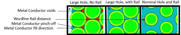
Figure 1: Top-Down View of Virtual-Model Experimental Runs. Each run (A, B and C) has different experimental conditions. A) Large memory cell hole size, no wordline rail, and voids enabled in the model. The voids in the wordlines are shown in red, with the voids creating a pinch-off caused by the small distance between the memory cell holes. B) Large memory cell hole size, nominal wordline rail distance, and voids disabled in the model. C) Nominal memory cell hole size, nominal wordline rail distance. The nominal wordline rail distance is illustrated in Image C.
We recently used a SEMulator3D model to better understand the factors impacting wordline resistance in 3D NAND. Our study indicated that 3D NAND wordline resistance was much greater than the calculated resistance that one would expect solely due to the removal of conductive material in the memory cell holes. Our study indicated that voids were being formed during the removal and replacement of the sacrificial silicon nitride with conductive metal, which added to wordline resistance. The SEMulator3D virtual models revealed that if the memory cell holes were too large, or the spacing between the holes was too narrow, the lateral deposition path to the interior regions of the wordline would be pinched-off and form voids in the conductive metal (Figure 2).
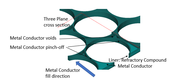
Figure 2: SEMulator3D Virtual Model showing the edge of a wordline in a three-plane cross section. The metal conductor fill does not continue past the pinch-off from the slit trench edge to the center of the wordline. Electrical current will only be conducted in the liner from the wordline center to the pinch-off.
We ran 200 virtual model experiments using our SEMulator3D process model, varying the Memory Cell Hole Diameter, Rail Distance and Void Tracking. The wordline resistance was simulated using the SEMulator3D Electrical Analysis package. Wordline resistance was then extracted from the virtual model experiments, and the percentage increase in resistance was plotted compared to Rail Distance, Memory Cell Hole increase and Void Tracking (Figure 3).
The effect of void formation on wordline resistance can be seen in Figure 3. If you compare the increase in wordline resistance without voids (red line) to the case where voids are present (blue line), the effect of voids is readily seen. The presence of voids increases the wordline resistance by 55%, independent of the memory hole size. Increasing the outer rail distance can reduce the effect of memory cell hole size on wordline resistance by 200%, and reduce the effect of void inclusion on wordline resistance to a negligible increase. The results demonstrate that wordline resistance increases with memory hole size.
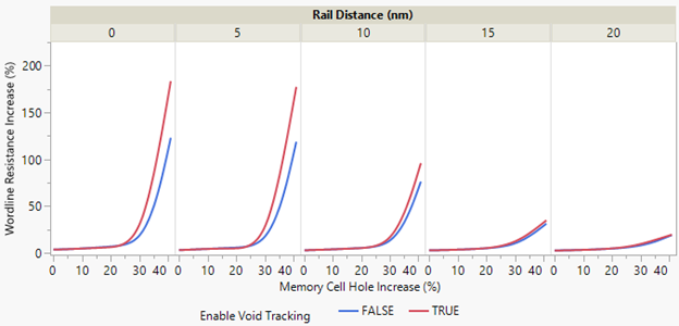
Figure 3: Wordline Resistance Increase (in percent) as a function of the Memory Cell Hole Diameter Increase (in percent) and Rail Distance (nm). The red line shows the result of including wordline voids in the model (TRUE) and the blue line deletes the wordline voids and fills them (FALSE).
As the rail distance approaches zero, more current is forced to flow through the internal region of the wordline. When the memory hole size increases, the voids increase in size and reduce the volume between the low resistance conductive metal and the higher resistance refractory compound liner (Figure 4). When wordline rail distance is preserved, the dependence of the wordline resistance on memory hole size and metal voids is minimized.
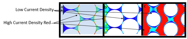
Figure 4: Current Density Top-Down View of Virtual-Model Experiment Runs. Each experimental setup (shown in Images A, B and C) have different experimental run treatments (refer to Figure 1 for treatment descriptions). Image A: The rail is not continuous, causing the current to flow through the interior of the wordline. Image B: The memory hole size is the same as in Image A, but the wide rail allows current to flow along the outer edges of the wordline. Image C: A nominal memory cell hole size is shown. In this case, the nominal wordline rail distance supports a more uniform current density pattern.
Using SEMulator3D Void Tracking, the virtual model was able to predict the effect of a void on wordline resistance, independent of the memory hole size. In actual silicon wafer processing, it is practically impossible to create an experiment where you decouple void formation and memory cell hole size during 3D NAND development. In SEMulator3D, experiments that would be difficult or impossible to perform in a fab become possible.
In conclusion, SEMulator3D process modeling was used to replicate a 3D NAND replacement gate wordline formation process. We learned that the upstream memory cell hole module can negatively impact the downstream wordline formation module, and create an extreme increase in the wordline resistance. Using the virtual model, we were able to simulate the problems between the upstream and downstream modules and run experiments to determine a potential solution (in our case, the solution would involve a layout modification). SEMulator3D process modeling can identify process and layout problems early in development without substantial silicon wafer experimentation, reducing development delays, wafer fabrication costs and time to market.
References:
- Handy, “An Alternative Kind of Vertical 3D NAND String”, Jim Handy, Objective Analysis, on Semiconductor Memories, Nov 8, 2013.
- A. Goda, “Recent Progress on 3D NAND Flash Technologies”, Electronics2021, 10(24), 3156.