When I was a small child, I remember watching a 1966 American sci-fi adventure movie called “Fantastic Voyage” (the Korean title was “Micro Squad”) on an old black-and-white TV. The special effects extravaganza and brilliant, thrilling plot had a huge impact on me at a young age. After more than 40 years, I still can’t get some of the surreal scenes out of my head.
In case you haven’t seen the movie, let me tell you the plot. A brilliant scientist has developed a revolutionary technology that could change the world. Unfortunately, the scientist has a blood clot that is going to kill him. To save the scientist, a team of researchers and their nuclear submarine are shrunk down to microscopic size and injected into the scientist’s bloodstream. The submarine’s crew has a finite amount of time to find and fix the blood clot, and leave the scientist’s body before the miniaturization effect wears off. The crew faces many obstacles and difficulties during their mission-critical journey. By the time that the crew finally reaches the blood clot, they only have 6 minutes left to operate on the clot and exit the scientist’s body. They succeed in removing the blood clot, and escape through a tear duct only seconds before returning to normal size.
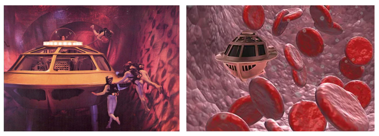
Courtesy: Twentieth Century – Fox Film Corporation
Modern, advanced semiconductor devices are already quite small, and they are getting smaller every year. The critical dimension we’re talking about are typically measured in nanometers or even angstroms. So, these devices are a fraction of the size of the objects represented in the movie (in the Korean title, “micro” refers to the size of a red blood cell, about 6 – 8 microns in size).
In the early stages of semiconductor development, we tackle nanoscopic “defects” or “failures” in semiconductor devices to make them free of defects and manufacturable in mass volume. During this early stage of development, a significant amount of time and money is expended to discover and remove these defects and make the device “healthy” (potentially far more time and money than the cost of a miniature submarine and its crew!).
In the movie, the submarine’s crew locates the problem and navigates to its position in order to eradicate the problem. All of this takes place in a real human body, and the crew cannot make any mistakes. If they do, they will not only kill themselves but also kill the patient and destroy the knowledge that could change the world. In the movie, there is no such thing as “error recovery” or “trying again.”
In the case of semiconductor development, it is possible to recover from a failure or defect when manufacturing a silicon device. However, it is very expensive to do so in terms of time and cost (and possibly a company’s reputation). Nobody wants to run tens or hundreds of repetitive wafer experiments to determine the cause of a failure or defect, or to have to solve the problem in a series of expensive DoE (Design of Experiment) tests. Furthermore, some failures or errors are difficult to resolve without destroying the device through reverse engineering or by de-capping the device (removing the outer layer to expose the silicon inside).
During destructive measurement, it is also inevitable that inaccuracies will be introduced into the measurement process. In addition, while many non-destructive inspection technologies (such as optical scatterometry) have become more accessible, they are not always able to measure and identify the fundamental cause of every device defect or failure.
Using virtual fabrication (process modeling) and analysis techniques, we can locate failures and defects without fear of destroying the “patient”. We can navigate inside the nanoscale device world to not only identify a defect in front of our eyes, but also determine its cause, the source of the problem and how it should be “treated”. In this crucial mission, you don’t have to put your life on the line. All you need is to have a computer (your normal PC) and some excellent software (SEMulator3D®) to start. Lam Research is now supplying that software to the entire semiconductor industry.
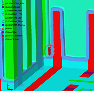
Figure 1: Undesirable poly-silicon residual fragments visible after a FinFET sacrificial gate wet etch process. The fragments were created due to a pattern loading effect.
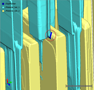
Figure 2: A FinFET electrical failure caused by a source/drain contact short at the tungsten gate. The root cause of this failure was mask misalignment.
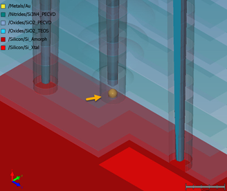
Figure 3: In a 3D NAND, a small point defect at the bottom of an ONON stack can magnify itself as the stack is deposited, and end up blocking a channel in the device.
Figure 4: A 3D NAND FG-FG distance violation was identified, which makes the device susceptible to shorts. The error was introduced due to the effects of etch bowing, lithography CD and mask overlay.
Now, let’s look at some similarities and differences between the mission in the movie and in using process modeling software.
Similarities
- Navigate and confront problems (clots or defects)
- Visually confirm the problem
- Find the root cause directly
- Solve the problem immediately
Differences
| Fantastic Voyage | Process Modeling using SEMulator3D |
|---|---|
| Your mission: Save a life | Your mission: Save a product (or maybe your company) |
| You are resolving “micro” scale defects | You are resolving “nano” scale defects |
| There is only one chance to save the patient | You can run simulations repeatedly, at any time, without harm or cost to the “patient”. |
| You only have 1 hour to finish the mission and survive | You can work on solving the problem as long as you have a software license (years!) |
| If you fail in your mission, you die | If you fail in your mission, don’t panic. It is only a simulation. |
Incidentally, if you choose to accept this fantastic voyage into semiconductor process development, don’t forget to record a movie in SEMulator3D so that you can play the role of the hero.