Introduction
As we approach the 1.5nm node and beyond, new BEOL device integration challenges will be presented. These challenges include the need for smaller metal pitches, along with support for new process flows. Process modifications to improve RC performance, reduce edge placement error and enable challenging manufacturing processes will all be required. To address these challenges, we investigated the possibility of using a semi-damascene approach with self-aligned patterning for BEOL at the 1.5nm node. A new BEOL device integration mask set was produced at imec for electrical evaluation of single damascene and dual damascene modules. The new mask set had metal pitches of 14nm and16nm (the target minimal metal pitch for the 1.5nm node BEOL), along with 18nm, 20nm and 22nm metal pitches. The latter allowed for process window assessment.
The Coventor SEMulator3D® virtual fabrication platform was used to describe the next generation semi-damascene process flow and also to investigate process assumptions and challenges of BEOL device integration using the new mask set. Additional process boosters to improve RC performance and improve manufacturing were also simulated and tested using the new mask set.
Semi-damascene approach with self-aligned patterning
A semi-damascene approach with self-aligned patterning was proposed, using a gap fill option and a spacer pull option.
The spacer pull option needs a selective etch process. Area selective deposition (ASD) was the best deposition choice for filling the LE2 gap. Figure 1 (a) displays a cut profile of the gap fill process, along with the position of spacers and the LE1 Core in the approach. SEMulator3D software was used to better understand the challenges of both the gap fill option and spacer pull option.

Figure 1: Gap fill and spacer pull options for 1.5nm node patterning process.
Semi-damascene process flow
SEMulator3D virtual fabrication was also used to simulate the semi-damascene process flow. Figure 2 depicts the process flow developed using simulation. Metal 2 was patterned using an SALELE option, and connected to printed metal 3 using EUV lithography. The simulated process flow was then used to perform sensitivity analysis of Metal 2 patterning and the Metal 2 to Metal 3 connection.
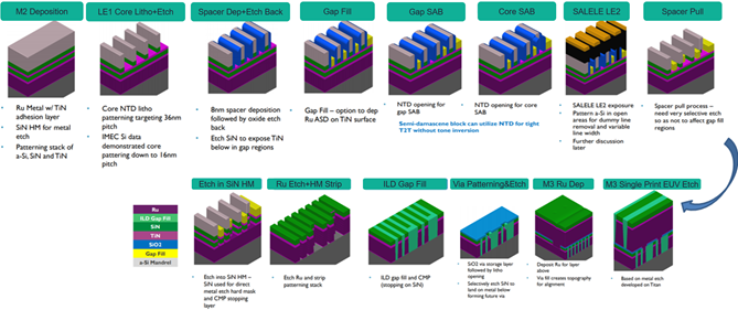
Figure 2: A semi-damascene process flow for BEOL device integration using the new mask set
Boosters
Figure 3 describes the process boosters which were also enabled on the new mask set. Using SEMulator3D, these mask set process boosters were also simulated and analyzed for feasibility and performance.
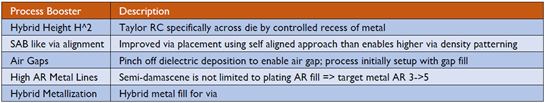
Figure 3: 1.5nm node process boosters which were enabled on the mask set
Hybrid Height
By tailoring the height of metal lines, we can fully optimize RC performance (Figure 4). This flexibility in metal line height is possible using etched direct metal lines. Tall metal lines have low resistance and high capacitance and might be beneficial for power lines and long signal lines. Short metal lines have high resistance and low capacitance and might be most beneficial for signal lines. Preliminary analysis of this concept was evaluated using Coventor SEMulator3D.
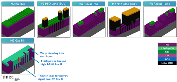
Figure 4: Hybrid height tailoring for optimized RC product performance
SAB like vias
Self-aligned patterning technology was first introduced at the 14nm node for interconnect technology. Self-aligned patterning creates parallel metal lines that need to be cut to produce functional devices. The edge placement error (EPE) for this cut mask is challenging, and at the 10nm and 7nm nodes a self-aligned block technology was developed to extend overlay tolerance to ¾ pitch. At the 1.5nm technology node, we expect this self-aligned technology will need to be extended to the via layer as the edge placement error (EPE) will be extremely challenging. Coventor SEMulator3D was again used to investigate different options for via self-alignment at the 1.5nm node (Figure 5).
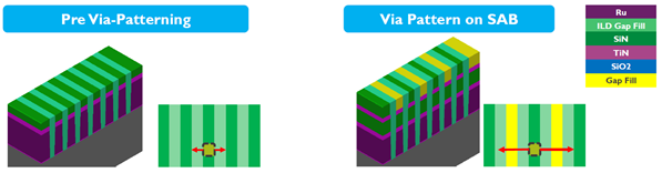
Figure 5: Semi damascene self-aligned via to improve via overlay alignment
Air Gaps
Air Gaps have been introduced for damascene, but require an additional etch step to remove ILD. For direct metal etch, the ILD is deposited at the end of the process. It is possible to target a deposition process that pinches off SiO2 at a tight pitch, resulting in air gap formation. Basic modeling of the formation of air gaps was explored in simulation, with additional simulation projects planned. In the initial process flow, we modeled a simple air gap fill followed by an oxide gap fill and CMP. We simulated this process flow using SEMulator3D (Figure 6).
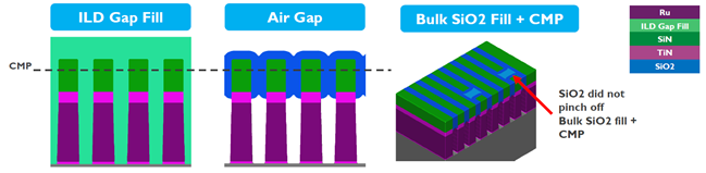
Figure 6: Airgap process formation simulation.
High AR Metal Lines
For traditional damascene, the aspect ratio is typically limited to ~ 2. Beyond this aspect ratio, it is difficult to deposit metal lines without void formation. With direct metal etch, the metal height is limited by the etch process and an aspect ratio of 5 or even greater is possible. This is an important process booster for advanced nodes, as the resistance increases with reduced dimensions. Increasing metal height is an important way to continue resistance scaling. A key challenge for a direct metal etch process is to reduce hard mask consumption during the etch. We modeled this challenge using Coventor SEMulator3D.
Hybrid Metallization
It is possible to use different metals for the lines and the vias. This can be done to reduce overall resistance, and is being explored by imec as part of their future studies.
Conclusions
Coventor SEMulator3D was used to define and simulate a BEOL process flow at the 1.5nm node and beyond. Based upon the results of these simulations, design rules were established for a new mask set. The mask set was successfully taped out using the process flow recommended during simulation. Performance boosters such as fully self-aligned vias, high aspect ratio metal lines and air gaps were also demonstrated in silicon, with the original IP for these concepts developed using SEMulator3D simulation. The results of these simulations have guided advanced node development activities at imec, with actual results in silicon.
Acknowledgment
The author gratefully acknowledges Martin O’Toole and imec for sharing this work with Coventor.
This research was supported by IT2 ECSEL Joint Undertaking.