With decreasing dynamic random-access memory (DRAM) cell sizes, DRAM process development has become increasingly difficult. Bit-line (BL) sensing margins and refresh times have become problematic as cell sizes have decreased, due to an increase in BL parasitic capacitance (Cb). The main factor impacting Cb is the parasitic capacitance between the BL and the node contact (CBL-NC) [1]. To reduce CBL-NC , low k spacers and airgap spacers are optional structures that have been proposed for use in DRAM memory cell architecture.
Si based experimentation could be used to evaluate new process integration schemes for these low k and airgap spacer structures, but this can be time-consuming and costly in practice. In this work, we will demonstrate how virtual fabrication can be used to evaluate new process integration schemes to reduce DRAM bitline parasitic capacitance [2]. We will review a simulation study of CBL-NC using a Nitride-Oxide-Nitride (NON) spacer and evaluate the improvement in using either a low k spacer or an airgap spacer. The purpose of this analysis is to obtain a quantified comparison between various integration schemes (NON/low k/airgap spacer integration schemes) and to provide clear guidance for process developers.
Process flow and virtual metrology description
Virtual structures were built using the SEMulator3D® virtual fabrication platform. Fig. 1 displays the final structure using a NON spacer (a), low-k spacer (b) and airgap spacer (c). The NON spacer consists of a Nitride-Oxide-Nitride structure. The low k spacer replaces Nitride (SN) with a low k, formation low k-Oxide-low k spacer structure. The airgap spacer is created by etching a dummy oxide (OX) spacer to form a Nitride-air-Nitride spacer structure. After the virtual structures were built, capacitance extraction was performed to evaluate the CBL-NC performance using different process integration schemes.
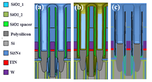
Fig. 1: (a) NON, (b) Low k and (c) Airgap spacer
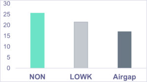
Fig. 2: CBL_NC in different integration schemes
Results
Figure 2 displays the extract capacitance results using our selected integration schemes. The low-k bit-line spacer integration scheme improves C BL_NC by about 16% compared to the original NON bit-line spacer. The airgap spacer integration scheme improves C BL_NC by about 33% compared to the original NON spacer configuration.
Conclusion
In this study, virtual fabrication was used to evaluate different process integration schemes to reduce bit-line parasitic capacitance in an advanced DRAM structure. The virtual evaluation provided clear and quantified guidance to help guide developers in their choice of integration schemes that can improve parasitic capacitance in an advanced DRAM structure.
References
[1] Q. Han, M. Cai, B. Wu and K. Cao.2020 IEEE 15th International Conference on Solid-State & Integrated Circuit Technology (ICSICT)2020, pp. 1-3.
[2] Q. Wang, Y. De Chen, J. Huang, B. Vincent and J. Ervin. 2022 China Semiconductor Technology International Conference (CSTIC)2022, pp. 1-4.