Introduction
BEOL metal line RC delay has become a dominant factor that limits chip performance at advanced nodes [1]. Smaller metal line pitches require a narrower line CD and line-to-line spacing, which introduces higher metal line resistance and line-to-line capacitance. This is demonstrated in Figure 1, which displays a simulation of line resistance vs. line CD across different BEOL metals. Even without line edge roughness (LER), the graph shows that resistance exponentially increases as line widths shrink [2]. To alleviate this problem, metal line CD optimization and careful metal material selection are required at smaller nodes.
Line edge roughness is also an important factor in determining electron surface scattering and subsequent line resistivity. Figure 1 (b) displays a scanning electron microscopy image of a typical 5 nm BEOL M2 line with visible LER [3]. Using virtual process modeling, we recently investigated the impact of LER on line-resistance, by varying RMS amplitude, correlation length, materials used and metal line CD.
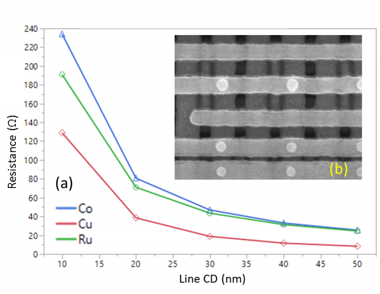
Figure 1: (a) Line resistance vs line CD, (b) a SEM top view of 5 nm M2 (Courtesy from TechInsights).
Experimental Design and Execution
In a fab, it is difficult, expensive and time-consuming to perform LER variation experiments by varying line CDs and metals. On a Si wafer, control of LER is also difficult due to lithography and etch process variability and limits. In these circumstances, virtual fabrication may be a more direct and effective way to “virtually” generate replicas of actual LER metal line structures and to calculate resistivity across a host of variables [4].
Figure 2(a) shows a layout design to simulate LER using a virtual process modeling platform (SEMulator3D®). Figures 2(b) and 2(c) display the resulting virtually fabricated structures and their simulated LER, from both a top view and a cross-sectional view. The LER can be modified directly in the lithography step of virtual fabrication by setting specific RMS amplitude (noise amplitude) and correlation lengths (noise frequency) values. Figure 2 (d) displays a simple split experiment of different LER conditions. Line edge roughness is displayed as a function of different metal line CDs, RMS amplitude and correlation lengths. This data was generated during a virtual Design of Experiments (DOE) in SEMulator3D. To systematically investigate the impact of line edge roughness using different CDs and materials, experimental splits were completed using the split conditions shown in Table 1. The corresponding metal line resistance was then extracted from the simulation results. For simplicity, liner material was not considered when simulating these structures.
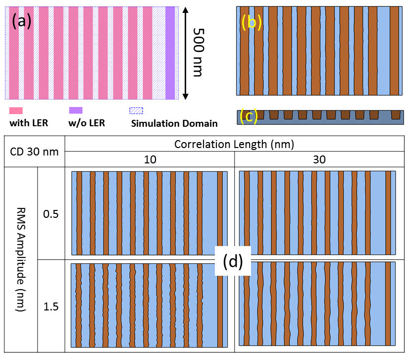
Figure 2: (a) Layout design, (b) Top view of a typical metal line generated, (c) cross sectional view of the metal line, (d) LER status of RMS and Correlation length split.

Table 1: DOE split conditions.
DOE Results and Analysis
More than 1000 virtual DOE experiments were completed using the split conditions from Table 1, to understand the impact of LER on metal line resistance. During these experiments, we learned that:
- Resistance is strongly impacted by LER when the correlation length is small and high-frequency noise is present.
- At smaller line CDs, resistance is affected by the LER RMS amplitude and correlation length.
- Specific metals should be chosen to obtain the lowest absolute resistance value during all Line CD and LER conditions.
Conclusion
LER control will become increasingly important at advanced nodes, since LER has a strong impact on resistance at smaller metal line CDs. We investigated the impact of LER on metal line resistance by varying metal line CDs and metal line materials during process modeling split experiments.
During EUV lithography, CDU and LER can be problematic due to the high testing cost and low energy density of most EUV tools. Under these circumstances, modifications to lithography development may be required to minimize LER. These modifications can be tested virtually, to lower the cost of development. New EUV resist approaches (such as the dry resist proposed by Lam Research®) may also help decrease line edge roughness at lower EUV exposure energy.
At advanced nodes, proper choice of metal line materials, CD optimization, and resist development will all be required to reduce LER and line resistance caused by electron surface scattering. Additional LER improvements (post lithography) may also be needed at future nodes to reduce LER-induced resistance.
References
- Chen, H. C., Fan, S. C., Lin, J. H., Cheng, Y. L., Jeng, S. P., & Wu, C. M. (2004). The impact of scaling on metal thickness for advanced back end of line interconnects. Thin solid films, 469, 487-490.
- van der Veen, M. H., Heyler, N., Pedreira, O. V., Ciofi, I., Decoster, S., Gonzalez, V. V., … & Tőkei, Z. (2018, June). Damascene benchmark of Ru, Co and Cu in scaled dimensions. In 2018 IEEE International Interconnect Technology Conference (IITC) (pp. 172-174). IEEE.
- Techinsights TSMC 5nm logic tear down report.
- SEMulator3D - Lam Research