Introduction
The semiconductor industry has been focused on scaling and developing advanced technologies using advanced etch tools and techniques. With decreasing semiconductor device dimensions and increases in process complexity, the impact of etch variation during the manufacturing process can be pronounced. Etch endpoint detection is used to determine when an etch process is complete and there is no more material left to etch. This type of endpoint detection can help minimize etch rate variability. Etch endpoint detection is accomplished through sensor and metrology measurements made during the etch process. When a specific sensor measurement or threshold is seen, the etch tool can be instructed to halt the etch operation. Reliable endpoint detection is important during the etch process, since the underlying material (or possibly the entire device or wafer) can be damaged if there is no more material to be etched, greatly impacting yield [1]. The semiconductor industry relies on metrology tools that provide critical information for process monitoring and control during the etch process. Both standalone metrology tools and in-situ (built-in) sensor-based metrology are now being used during wafer etch processing to improve yield. In-situ metrology has an advantage over standalone metrology since it allows etch-related processes (such as the etch end-point detection) to be monitored and controlled in real-time.
Etch Endpoint Detection Using SEMulator3D® Process Steps
SEMulator3D can be used to model in-situ etch end point detection, by building a series of “virtual” processes containing a virtual etch step, variables, sequences, and loops. Sequence looping is used to repeat process steps over a fixed amount of time, providing flexibility in process flow control (such as automatic process control) [2]. To model a control sequence, a certain number of loops can be set using a “For Loop” or an “Until Loop” (just like in computer programming). For etch endpoint detection, one can use an Until Loop since the condition is met that no material is left to etch. In the loop, the user can identify how many loops have occurred with the help of a loop index. In addition, SEMulator3D has the ability to perform “Virtual Metrology” to help track the thickness of the material during the etch process loop and provide real-time updates regarding material thickness. Combining both the virtual metrology film thickness measurement and the loop index of the sequence, one can accurately acquire in-situ material etch depth measurements after every loop.
SEMulator3D Example for Etch End Point Detection
Initial Setup
In a simple example, four fins in a dense region along with an isolated area to the right of the dense region are shown in our layout image (see Figure 1). We would like to measure the etch depth in the dense region when the isolated area runs out of material. The area that we will use for modeling is shown in the blue box, where there are four fins (shown in red) to manufacture. In addition, we have yellow and green metrology box measurement areas where we will measure the film thickness of the isolated region (MEA_ISO_FT) and the etch depth of the trench region (MEA_TRENCH_FT) respectively. Our process flow begins with a wafer setup using a 20nm thick silicon crystal layer (red), 30nm of oxide (light blue), and 10nm of photoresist (purple) (Figure 2). We expose the fins and use a multi-etch process to etch the fins. We are using a basic etch on the resist, and a visibility etch with a defined source directionality on the oxide material. Our selectivity is 100 to 1 for oxide to resist. We are using a visibility etch model in SEMulator3D to see if there is a difference in thickness between the isolated region and the dense regions with the fins.
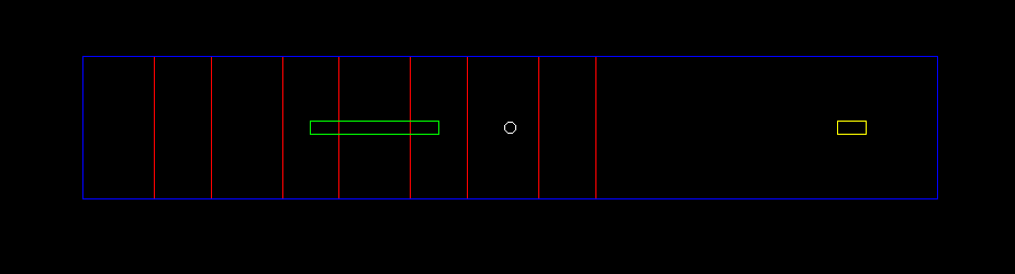
Fig 1: Model bounding area (blue) with four fins (red) and 2 metrology boxes used to measure the film thicknesses of the isolated region (yellow) and trench region (green).
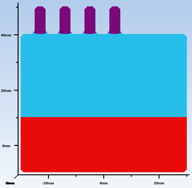
Fig 2: SEMulator3D Model with silicon crystal (red), oxide (light blue) and four fins developed in photoresist (purple).
SEMulator3D Etch Endpoint Detection Looping
The process flow in SEMulator3D is configured using a looped sequence with an until loop. We will measure the material thickness in the isolated region, and stop the process once the isolated oxide film thickness is exhausted (MEA_ISO_FT==0). Within this loop, we will execute our multi-etch process against the oxide material every 1 nm (the model resolution), while we measure the isolated region oxide film thickness. In addition, we will keep track of the etch depth within the trench region between 2 of the fins after every loop. This loop index helps to keep track of the number of the iterations in the multi-etch loop (Figure 3).
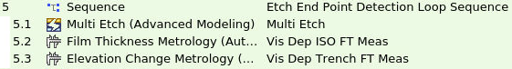
Fig 3: Looped sequence in SEMulator3D for etch end point detection
Results
Figure 4 displays the model results as material is etched through the isolated film until it has a remaining depth of 20 nm, 10 nm and 0 nm. The isolated film thickness measurements are calculated in the model, as well as the etch depth within the trench region between the two fins.
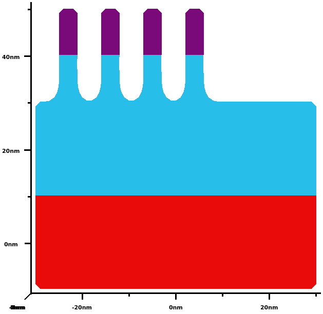
Fig 4a-c: Process model flow of film thickness at the isolated region of a) 20 nm, b) 10 nm and c) 0 nm with corresponding trench etch depth from bottom of resist.
As we perform almost 30 iterations of the looping model, we see that the isolated region film thickness now has reached zero and we can track the trench region oxide etch depth (28.4 nm of the 30nm of oxide in the dense region is gone, when the isolated region has been fully etched).
Conclusion
SEMulator3D can be used to create a virtual model of an etch end point detection process. This technique can be used to determine what material has been completely removed during the etch processes, and can also measure material that is left over after the etch (depending upon the type of etch). Using this methodology, modeling of in-situ etch depth control can be successfully pursued. Other types of automated process control such as DRIE etching or HDP-CVD process control can also be undertaken using a similar methodology.
References:
- Derbyshire, Katherine. In Situ Metrology for Real-Time Process Control, Semiconductor Online, 10 July 1998, https://www.semiconductoronline.com/doc/in-situ-metrology-for-real-time-process-contr-0001.
- SEMulator3D V10 Documentation: Sequences, Loops, Variables, etc.