With continuous device scaling, process windows have become narrower and narrower due to smaller feature sizes and greater process step variability [1]. A key task during the R&D stage of semiconductor development is to choose a good integration scheme with a relatively large process window. When wafer test data is limited, evaluating the process window for different integration schemes can be difficult. To overcome this limitation, we will discuss an example of how virtual fabrication can be used during process window evaluation of a DRAM capacitor patterning process.
When developing a DRAM device, an array of holes used for capacitive charge storage must be etched into the silicon wafer. The available patterning schemes to manufacture a 40 nm hole array include EUV LE, LE4, double SADP (80 nm mandrel pitch), and double SAQP (160 nm mandrel pitch). In this study, we selected immersion double SADP and SAQP for our patterning schemes and compared the process sensitivity and process windows of our selections. A virtual process sequence (“flow”) was built for each patterning scheme (SADP and SAQP) as shown in Figure 1. We used the capacitor hole area as a metric for the capacitance and its uniformity analysis. Structure search was used in SEMulator3D to find the minimum and maximum capacitor hole area within a 4×4 hole array, and then calculate the mean area, so that the delta from maximum to minimum area could be calculated. Figure 2 displays the metrology results for one output structure, with the minimum and maximum hole areas identified.
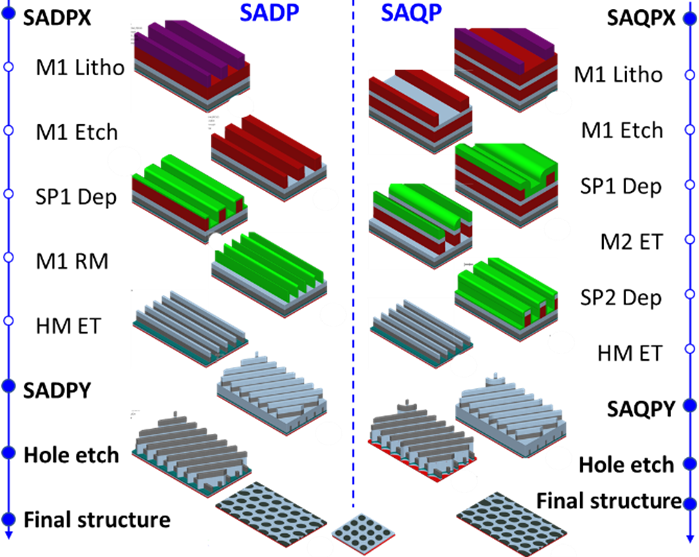
Figure 1. Major process steps of SADP and SAQP
.png)
Figure 2. Virtual metrology results for minimum and maximum area.
Based on this virtual flow and metrology, a Monte Carlo study with 3000 trials was performed using the SEMulator3D Analytics module. Mandrel CDs and spacer thicknesses were selected as Design of Experiment (DOE) input parameters, while mean area and delta area were selected as the output parameters. Table 1 lists the ranges of input parameter values for the SADP and SAQP processes. The virtual DOE results guided our investigation regarding the impact of each input on variations in the mean and delta area. In Table 1, MX is the X direction mandrel CD; MY, the Y direction mandrel CD; SPX1, the X direction 1st spacer thickness; SPX2, the X direction 2nd spacer thickness; SPY1, the Y direction 1st spacer thickness; and SPY2, the Y direction 2nd spacer thickness.

Table 1: DOE variables and input ranges.
A larger mean area and smaller delta are preferred for a higher and more uniform capacitance distribution. A mean area between 900 and 1100 nm2 and delta smaller than 200 nm2 were defined as the success criteria that determined which trials passed or failed. The ratio of passed to failed simulation runs (known as the in-spec ratio) can be calculated for the process window under a specific set of conditions, to generate a mean value and 3-sigma (±3*standard deviation) distribution. This ratio indicates the fraction of input combinations that produce mean and delta areas within the success criteria ranges.
The in-spec ratio can be optimized by shifting the mean values of the input process parameters in order to maximize the number of successful runs included in the mean±3 sigma window [2]. If the optimized in-spec ratio is still not high enough, specification (3 sigma) tightening can further enhance it. We calculated In-spec ratio for both SADP and SAQP processes under different conditions. With the same 3 sigma distribution, the in-spec ratio of the SADP process was about 10% higher than that of the SAQP process. After the 3-sigma specification for the mandrel CD was modified, the in-spec ratio of the SADP process was close to 100%. The in-spec ratio was lower for the SAQP process at the same mandrel CD, highlighting that the SAQP process window needed further tightening.
In this study, virtual fabrication was used to perform process window evaluation and optimization for the capacitor formation process in an advanced DRAM structure. The virtual evaluation provided clear and quantified guidance to help gauge process difficulties in this advanced DRAM structure using different patterning schemes. Most importantly, we were able to determine optimal process target combinations and the largest allowable process window for each patterning scheme, prior to wafer-based experimentation.
Interested in learning more?
Full whitepaper “Pathfinding by process window modeling: Advanced DRAM capacitor patterning process window evaluation using virtual fabrication” ©2022 IEEE | DOI: 10.1109/CSTIC55103.2022.9856740
References
- A.J., Strojwas, 2006 IEEE International Symposium on Semiconductor Manufacturing (pp. xxiii-xxxii).
- Q. Wang, Y. D. Chen, J. Huang, W. Liu and E. Joseph, 2020 China Semiconductor Technology International Conference (CSTIC) (pp. 1-3).