Introduction
In logic devices such as FinFETs (field-effect transistors), metal gate parasitic capacitance can negatively impact electrical performance. One way to reduce this parasitic capacitance is to optimize the metal gate recess dimensions. However, there are limits to reducing this capacitance if you simply remove more of the metal material, since this can modify capacitance unexpectedly through changes in the metal gate recess profile. Varying the metal gate recess profiles, using sharp head or antenna configurations, could potentially help balance the resistance and capacitance values and improve electrical performance. We will now review the results of using SEMulator3D® virtual DOEs (Design of Experiments) to predict resistance and capacitance under different gate critical dimensions (CDs), metal gate recess depths and metal gate recess profiles.
Methodology
For this study, a 5nm FinFET process deck was assembled in SEMulator3D with a POR pitch of 44nm (see Figure 1, far left). The gate CD was set at 20 nm and the trench CD was set at 24 nm. To provide proper resistance values at different geometries, specific material properties for size correction were established for the TiN, TiAl and W metal liners. The SAC (self-aligned contact) Cap Nitride CMP (chemical mechanical polishing) step was kept at a constant over polish depth of 30nm once it hit a particular oxide. We varied the gate CD and W etch back step as part of our DOE in our metal gate recess profile study. To vary the gate CD, the dimensional bias in the X direction was modified by 1nm increments per side. Gate CDs varied from 6nm to 30nm in 2nm increments. For the W etch back (W ETB) step, the increments ranged from 25nm to 60nm in 5nm increments.
To measure resistance, resistance ports were established in our process model. We used a cut plane method to establish a port right at the NFET epi and PFET epi (see Figure 1, middle and far right). We then measured the resistance of the metal gate in between that space. In addition to these resistance calculations, we calculated the resistance with and without size correction. Size correction allows users to define resistivity in terms of model geometry. For this project, the size correction property of TiN was used for TiAl as well.

Figure 1: 3D Model of FinFET device, with cut plane (middle and far right) used for resistance measurements.
Results
We first observed the resistance change with respect to the gate CD, with and without size correction. The results are shown in Figure 2.
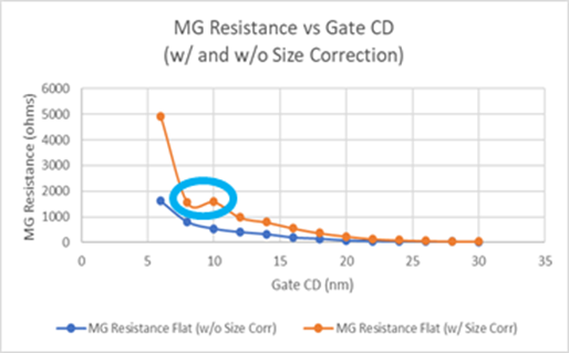
Figure 2: Metal Gate Resistance as a Function of Gate CD

Figure 3: NFET Cut View displays gate CD lengths (values from left to right of 26nm, 20nm and 10nm).
Next, we measured the resistance with respect to the metal gate recess depth in 5nm increments. The results indicate that the resistance did not vary at W etch back depths lower than 45nm, due to the use of an SAC Nitride Cap CMP over polish step.
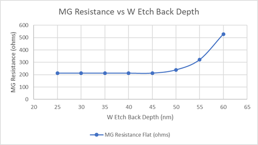
Figure 4: Metal Gate Resistance as a Function of Metal Gate Recess Depth (measured as W Etch Back Depth).

Figure 5: W Etch Back Depths (from left to right) of 60nm, 50nm 35nm. Images are taken after SAC Nitride Cap CMP step.
Once we reviewed the different gate CDs and W etch back depths, we then focused on varying the W etch back profiles. Two possible profiles (aside from the nominal profile) include antenna and sharp head profile shapes. The antenna shape mimics the profile of water held in a graduated cylinder. In this shape configuration, the W is etched deeper in the center of the gate than the TiN and TiAl at the edges. This might lead to a higher resistance compared to the nominal (consistent etch depth) profile. The sharp head profile can be thought of as a ball point pencil with more of the W preserved in the middle of the profile while the TiN and TiAl at the edges are etched deeper. This configuration could potentially lead to a lower overall resistance. We used pattern dependence on the etch back step to model these two profiles. Metal materials such as the TiN, TiAl and W were used to create a global mask in the step. The global mask uses dark and light polarity for the antenna and sharp head shape, respectively. Once the two new profiles (for the antenna and sharp head profiles) were created, the gate CDs and W ETB were varied, and the resistances were calculated by the same method described earlier (Figure 6).

Figure 6 (left to right): Different profiles using pattern dependence for the antenna and sharp head shapes. a) Antenna shape with POR flow (b) Antenna profile with a gate CD of 26nm (c) Sharp head profile with a gate CD of 28nm (d) Sharp head profile with an etch.
In the graphs shown below (Figure 7), the blue line displays resistance results for the original Gate CD profile (our original process of record (POR) shape), while the orange line displays results for the antenna profile and the gray line represents the sharp head profile. We see from Figure 7 that the resistance measurements for the 3 different profiles are almost the same over changes in gate CD. However, resistance measurements plotted against W etch back depth vary when the W etch back depth is greater than 50nm. The resistance values, shown from highest to lowest, are the antenna, flat and sharp head profiles.

Figure 7: Metal gate resistance vs gate CD (left) and metal gate resistance vs W Etch Back depth (right) with three profiles: flat (blue), antenna (orange) and sharp head (gray).
In the final step of this study, to complete our capacitance measurements, we first establish nets within our device. For this, the PFET and metal gate nets are created (see Figure 8). We then extract resistance and capacitance values for the nets. The resistance and capacitance measurements with respect to gate CD and W etch back depth are shown in Figures 9 and 10.
.
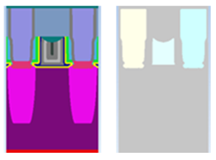
Figure 8: PFET cut showing the PFET to metal contact and metal gate nets for capacitance calculations.
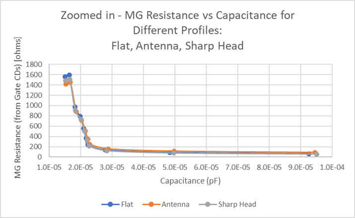
Figure 9: Metal gate resistance with respect to gate CD vs capacitance for the three different metal gate profiles: flat (blue), antenna (orange) and sharp head (gray).
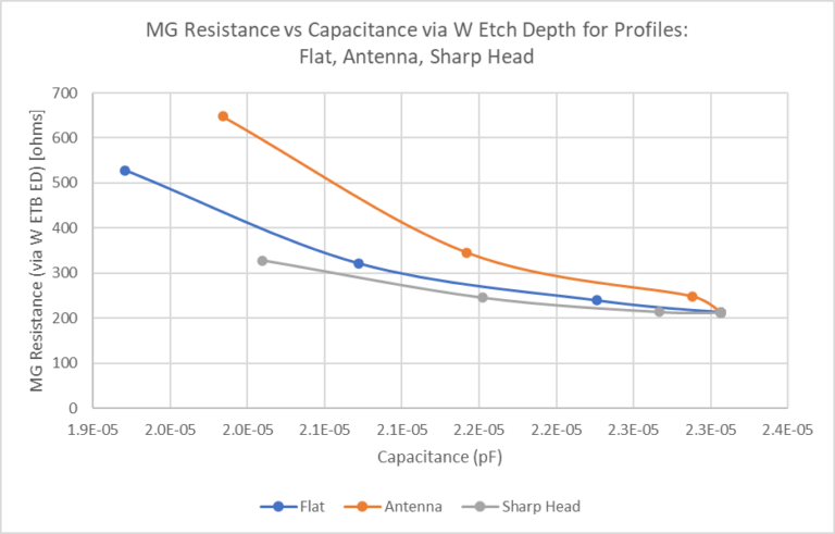
Figure 10: Metal gate resistance with respect to W etch back depth vs Capacitance for the three different metal gate profiles: flat (blue), antenna (orange), and sharp head (gray).
Our results indicate that there is little difference in R vs C values for the 3 different profiles when looking at resistance with respect to gate CDs. However, when we look at resistance versus capacitance with respect to the W etch back depth, we see that the sharp head recess profile has similar capacitance to the other profiles but lower resistance.
Conclusion
In this study, we used the SEMulator3D®’s Electrical Analysis, Pattern Dependence and Expeditor modules to calculate and better understand the impact of metal gate recess profile on resistance and capacitance. We were able to demonstrate that optimizing the metal gate CD profile can improve resistance and performance in a FinFET design.