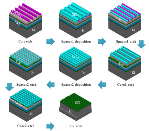
N7 FinFET Self-Aligned Quadruple Patterning Modeling
July 19, 2018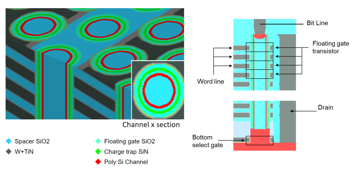
Innovative Solutions to Increase 3D NAND Flash Memory Density
January 25, 2019You must have an account on our Customer Portal to access this content. If you already have an account, please log in using the form below or to the right. If you do not have an account, we invite you to request an account.
Whitepaper: Effects of a Random Process Variation on the Transfer Characteristics of a Fundamental Photonic Integrated Circuit Component

To download your free white paper, please fill out the form below:
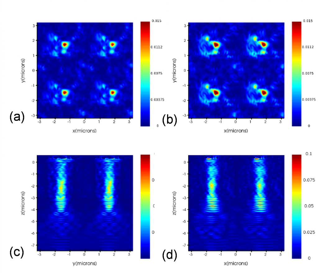
Silicon photonics is rapidly emerging as a promising technology to enable higher bandwidth, lower energy, and lower latency communication and information processing, and other applications. In silicon photonics, existing CMOS manufacturing infrastructure and techniques are leveraged. However, a key challenge for silicon photonics is the lack of mature models that take into account known CMOS process variations and their effect on photonic component behavior.
In this paper, the authors study the effect of a well-known random process variation, line edge roughness (LER), present in the lithography and etch process, on the performance of a fundamental silicon photonics component (the Y-branch) through virtual fabrication simulations. Ensemble statistical virtual fabrication and FDTD photonic simulations across a range of LER amplitude and correlation lengths are reported. These results indicate that component performance can be adversely impacted by random variations in the lithography and etch processes, depending on the statistical nature of the LER perturbations.
Sally I. El-Henawy, Ryan Miller, Duane S. Boning, "Effects of a random process variation on the transfer characteristics of a fundamental photonic integrated circuit component," Proc. SPIE 10743, Optical Modeling and Performance Predictions X, 107430O (17 September 2018); doi: 10.1117/12.2321515
© 2018 Society of Photo Optical Instrumentation Engineers (SPIE). One print or electronic copy may be made for personal use only. Systematic reproduction and distribution, duplication of any material in this publication for a fee or for commercial purposes, or modification of the contents of the publication are prohibited.
You might also be interested in:
- You must have an account on our Customer Portal to access this content. If you already have an account, please log in using the form below or to the right. […]