Modeling of Cross Wafer Induced Process Variations
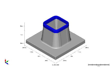
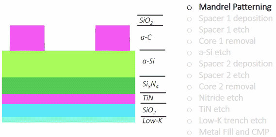
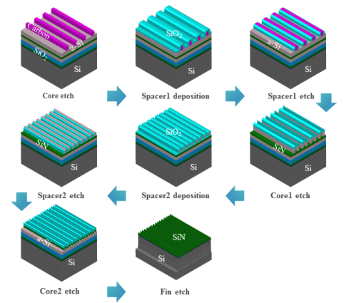
October 6, 2015Self-aligned quadruple patterning to meet requirements for fins with high density
May 20, 2016You must have an account on our Customer Portal to access this content. If you already have an account, please log in using the form below or to the right. If you do not have an account, we invite you to request an account.
Whitepaper: Defect Evolution in Next Generation, Extreme Ultraviolet Lithography

To download your free white paper, please fill out the form below:
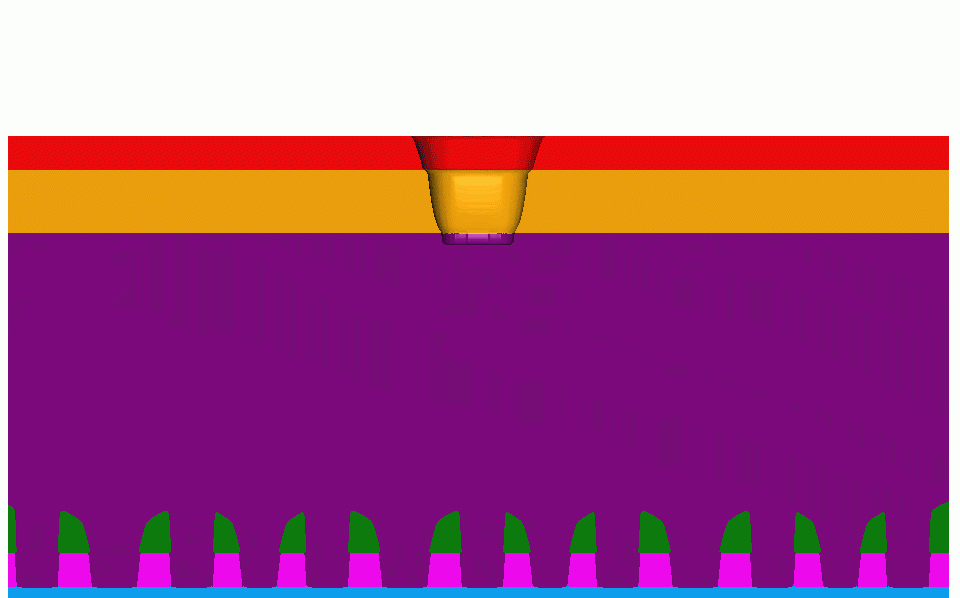
Extreme ultraviolet (EUV) lithography is a promising next generation lithography technology that may succeed optical lithography at future technology nodes. EUV mask infrastructure and manufacturing of defect-free EUV mask blanks is a key near term challenge in the use of EUV lithography.
Virtual fabrication is a computerized technique to perform predictive, three dimensional modeling of semiconductor fabrication processes. Virtual fabrication allows engineers to test semiconductor process changes and process variability in minutes or hours, instead of the weeks or months required to test their designs using actual semiconductor wafers. SEMulator3D is a virtual fabrication solution that can model process variability under complex patterning schemes and process flows.
In this study, SEMulator3D was used to predict mask defects and provide insight into the potential implementation of EUV lithography in high volume semiconductor manufacturing.
You might also be interested in:
- You must have an account on our Customer Portal to access this content. If you already have an account, please log in using the form below or to the right. […]
- You must have an account on our Customer Portal to access this content. If you already have an account, please log in using the form below or to the right. […]
- You must have an account on our Customer Portal to access this content. If you already have an account, please log in using the form below or to the right. […]
- You must have an account on our Customer Portal to access this content. If you already have an account, please log in using the form below or to the right. […]
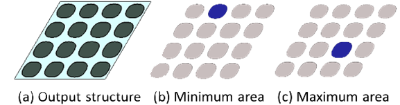
Impact of EUV Resist Thickness on Local Critical Dimension Uniformities for <30 nm CD Via Patterning
Impact of EUV Resist Thickness on Local Critical Dimension Uniformities for <30 nm CD Via Patterning
You must have an account on our Customer Portal to access this content. If you already have an account, please log in using the form below or to the right. […]- You must have an account on our Customer Portal to access this content. If you already have an account, please log in using the form below or to the right. […]
- You must have an account on our Customer Portal to access this content. If you already have an account, please log in using the form below or to the right. […]
- You must have an account on our Customer Portal to access this content. If you already have an account, please log in using the form below or to the right. […]
- You must have an account on our Customer Portal to access this content. If you already have an account, please log in using the form below or to the right. […]
- You must have an account on our Customer Portal to access this content. If you already have an account, please log in using the form below or to the right. […]
- You must have an account on our Customer Portal to access this content. If you already have an account, please log in using the form below or to the right. […]
- You must have an account on our Customer Portal to access this content. If you already have an account, please log in using the form below or to the right. […]
