Skip to main content
LOG IN
REGISTER
Home
Customer Portal
Coventor Licensing Downloads
SEMulator3D Downloads
CoventorMP Downloads
Webinars
MEMS+ Courses
System Requirements
Software Licensing
Contact Us
✕
Enter your search
(more…)
Modeling of Tone Inversion Process Flow for N5 Interconnect to Characterize Block Tip to Tip
Read more
- Modeling of Tone Inversion Process Flow for N5 Interconnect to Characterize Block Tip to Tip
Modeling of Tone Inversion Process Flow for N5 Interconnect to Characterize Block Tip to Tip
(more…)
Understanding how small variations in photoresist shape significantly impact multi-patterning yield
Read more
- Understanding how small variations in photoresist shape significantly impact multi-patterning yield
Understanding how small variations in photoresist shape significantly impact multi-patterning yield
(more…)
Optimizing DRAM Development using Directed Self-Assembly (DSA)
Read more
- Optimizing DRAM Development using Directed Self-Assembly (DSA)
Optimizing DRAM Development using Directed Self-Assembly (DSA)
(more…)
New Techniques to Analyze and Reduce Etch Variation
Read more
- New Techniques to Analyze and Reduce Etch Variation
New Techniques to Analyze and Reduce Etch Variation
(more…)
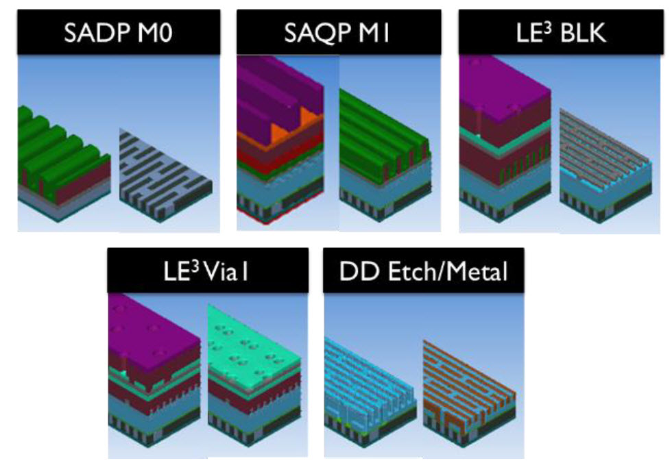
A million wafer, virtual fabrication approach to determine process capability requirements for an industry-standard N5 BEOL two-level metal flow
Read more
- A million wafer, virtual fabrication approach to determine process capability requirements for an industry-standard N5 BEOL two-level metal flow
A million wafer, virtual fabrication approach to determine process capability requirements for an industry-standard N5 BEOL two-level metal flow
(more…)
Self-aligned quadruple patterning to meet requirements for fins with high density
Read more
- Self-aligned quadruple patterning to meet requirements for fins with high density
Self-aligned quadruple patterning to meet requirements for fins with high density
(more…)
Defect Evolution in Next Generation, Extreme Ultraviolet Lithography
Read more
- Defect Evolution in Next Generation, Extreme Ultraviolet Lithography
Defect Evolution in Next Generation, Extreme Ultraviolet Lithography
(more…)
Modeling of Cross Wafer Induced Process Variations
Read more
- Modeling of Cross Wafer Induced Process Variations
Modeling of Cross Wafer Induced Process Variations
(more…)
3D NAND Flash Processing
Read more
- 3D NAND Flash Processing
3D NAND Flash Processing
(more…)
Load more
Contact Us
LOG IN
REGISTER
![3D NAND flash memory array, based on TCAT [1], with 16 cells per string, top gate-select layer and bottom source-select layer.](https://www.coventor.com/wp-content/uploads/2014/05/TCAT_whole_bf-M1-marked1.png)