Introduction
Cu’s resistivity depends on its crystal structure, void volume, grain boundaries and material interface mismatch, which becomes more significant at smaller scales. The formation of Cu wires is traditionally done by etching a trench pattern in low-k silicon dioxide using a trench etch process, and subsequently filling the trench with Cu via a damascene flow. Unfortunately, this method produces multi-crystalline structures with significant grain boundaries and voids, which increases the Cu wire resistance. A highly resistive TaN liner material is also utilized in this process to prevent Cu diffusion during the damascene annealing process.
Physical vapor deposition (PVD) can be used to deposit copper at high kinetic energies (between 10 to 100 eV), forming low resistance, dense single crystal structures. A drawback to PVD is that PVD deposition has a line of sight spread and can only be deposited uniformly on flat surfaces. It cannot be used to fill deep holes or trenches (Fig 1a). To form isolated wire shapes, a uniform Cu layer must be deposited on a flat surface and then physically etched by ion beams. Cu forms no volatile compounds with reactive gases, so a reactive ion etch process cannot be used. Accelerated Ar ions created during ion beam etch (IBE) can remove Cu if the incident angle is very high. Unfortunately, the etchable regions will be limited due to mask shadowing effects. Fig 1b shows the regions (in red) where material cannot be etched when the mask is perpendicular to the incoming ion beam. This etch failure occurs due to either shadowing or blockage of the path of the ejected atom. When the mask is parallel to the path of the ion, all unmasked regions can be etched. Thus, ion beam etching is limited to etching line shaped masks of arbitrarily long lengths.
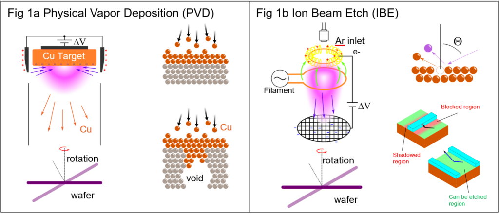
Fig 1a Physical Vapor Deposition (PVD); Fig 1b Ion Beam Etch (IBE)
Process Steps and Virtual Fabrication Process
In order to understand the effect of deposition and etch on line resistance, we now model the PVD and IBE etch processes using SEMulator3D® visibility deposition and etch functions. PVD was reproduced using a 30 degree angular spread visibility deposition process in SEMulator3D, which accurately models the random nature of ejected Cu atoms during bombardment with AR ions. IBE was reproduced in the model using a visibility etch with a 2 degree angular spread and a 60 degree polar angle tilt, to reflect the behavior of grid accelerated ions with low beam divergence. Both wafers are assumed to have free rotation. Other process steps have been adjusted in the virtual fabrication process to accommodate IBE and PVD constraints. Fig 2 displays the same structure created using both a damascene Cu fill (Figure 2a) and PVD/IBE process (Figure 2b). Additional process steps were included to incorporate certain limitations of PVD/IBE and create the equivalent shape for our desired end structures.
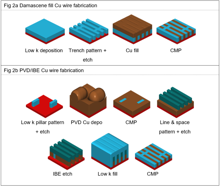
Fig 2a Damascene fill Cu wire fabrication;
Fig 2b PVD/IBE Cu wire fabrication
We then demonstrate that an equivalent 16 nm SRAM circuit cell can be fabricated with PVD/IBE wires while adhering to these limitations. Since all metal layers above the middle end of line are fabricated from a flat surface, this makes it an idea candidate for PVD/IBE wires, unlike the complex interconnect topologies seen in a FinFET device. Fig 3 displays the isolated structure of each metal layer, and the necessary steps needed to create a three metal layer FinFET structure using PVD/IBE.
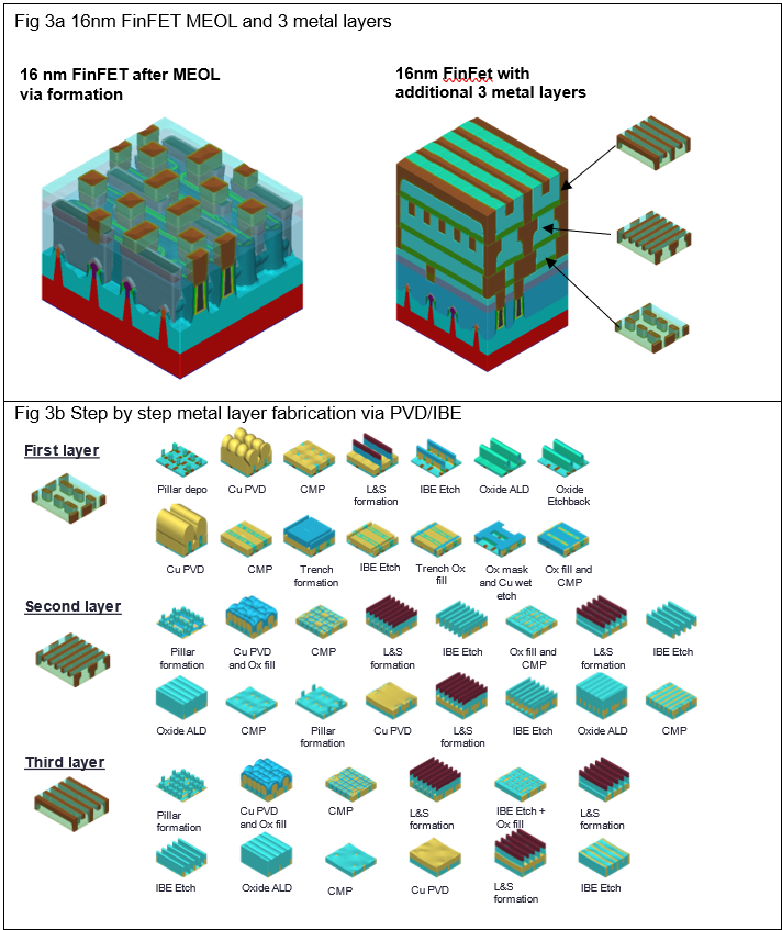
Figures 3(a) and (b) display the isolated structure of each metal layer, and the necessary steps needed to create a three metal layer FinFET structure using PVD/IBE. Figure 3(a): Two images are shown in this figure. The leftmost figure displays the completed MEOL 16nm FinFET structure while the right image shows the structure with 3 full metal layers. Right after the MEOL step is a flat topology where the Cu PVD and IBE can begin. Figure 3(b): This figure displays the step by step metal layer fabrication via PVD/IBE for the first, second and third metal layers. The process and integration pathfinding for the fabrication within PVD and IBE constraints of the 3 metal layers is demonstrated in Figure 3(b). The fabrication of each layer has images that display each process step in forming that layer. Each of the layers has some combination of pillar formation, CU PVD, CMP, L&S formation, oxide fill, IBE Etch, ALD, CU PVD and other individual process steps shown in the figure. To form separating wires, it is necessary to fabricate pillars and mesas which act as insulating barriers to separate wires. Then after the deposition has been flattened, a line and space patterning with an arbitrarily long etch in the X or Y direction forms the wire in the respective direction. To form vias, a crisscross etch is performed so that the intersection of line masks in the X and Y direction will be shielded from etching. Regions not needing vias can be suppressed by the placement of an insulating pillars prior to metal deposition.
Resistance Results and Conclusion
We then measure the electrical resistance of the wires from the top most metal layer down to the vias of the FinFET P and N channels, for both the damascene flow and physical vapor deposition. Fig, 4 shows the starting point and ending point of the resistance measurement at the P and N channels (all other insulating materials are transparent). To compensate for the interface resistance between the TaN liner and the copper wire, the resistivity of copper was increased by using an exponential decay constant of 1 nm as a function of the nearest distance to the TaN interface. Since a damascene fill Cu deposition is not expected to be fully crystalline, the resistivity of Cu was increased by 50%. The PVD/IBE copper process does not use a TaN liner, so the exponential decay function was not applied, and the bulk resistivity of copper was used in this model. A table of resistivity comparing a Damascene flow vs. PVD is included in Figure 4.
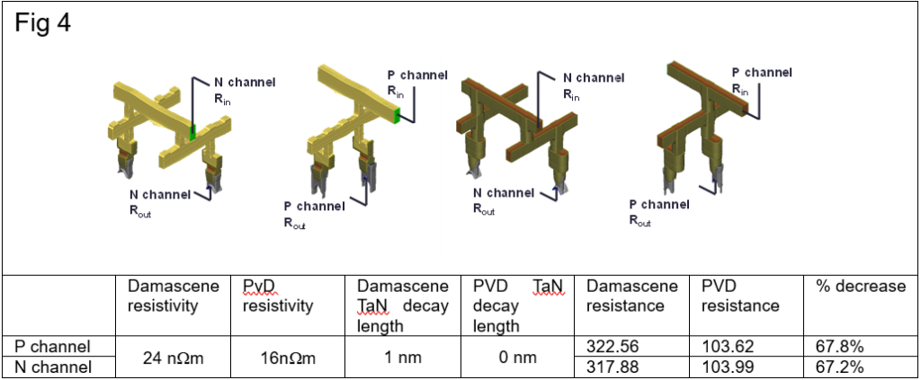
Figure 4 displays 3D models of FinFET devices using both damascene flow and physical vapor deposition processes. The models just display the points at which resistance is measured on the P and N channels. Underneath the 3D models, a table is displayed that compares the damascene and PVD resistance values for the P & N channels, with a 67% percentage decrease in resistance shown using IBE/PVD compared to damascene deposition.
The resistance values calculated from our model state that we can achieve a 67% decrease in resistance using the IBE/PVD fabrication method compared to a conventional trench etch followed by damascene deposition. This occurs since no TaN liner is needed in IBE/PVD and there is lower CU resistivity during this process. Our results indicate that resistivity improvements can be achieved by using IBE/PVD compared to damascene fill during metal line formation, at the cost of a more complex fabrication process.