Design of Experiments (DOE) is a powerful concept in semiconductor engineering research and development. DOEs are sets of experiments used to explore the sensitivity of experimental variables and their effect on final device performance. A well-designed DOE can help an engineer achieve a targeted semiconductor device performance using a limited number of experimental wafer runs. However, in semiconductor design and fabrication, the DOE (or experimental) space is usually not fully explored. Instead, very traditional trial and error methods are typically used to explore a limited experimental space. This is due to the fact that there are too many variables in the semiconductor manufacturing process to fully explore the entire design and manufacturing space. To explore the entire DOE space can require an extremely large number of wafer runs (with significant wafer costs and cycle time). This makes it unaffordable or unrealistic to fully explore all potential design and manufacturing alternatives. In these circumstances, virtual process models and virtual DOEs can be a valuable tool when exploring a large potential solution space, accelerating process development while reducing Si experimental cost. In this blog, we will provide an example of how we used a virtual DOE to maintain void control using bowing profile specifications for a via W filling process in a high aspect ratio device. In our example, the W fill process is performed using an in-situ deposition-etch-deposition (DED) methodology.
Based on Si SEM images and the basic behavior of each filling step, a via W filling process was reconstructed using SEMulator3D® virtual process modeling. The modeled processes included: 1) an Incoming trench etch (BT, BTOE, ME, OE), 2) a DED process (1st deposition, 1st depth dependent etch, 2nd deposition process), and 3) void tracking and virtual measurement of the void volume. Each step was calibrated in the process model to match the actual Si profile. The simulated 3D output structure generated using SEMulator3D closely corresponded to the Si images, with similar void location and void volume (see Figure 1). Figure 1 displays each equivalent process step in SEMulator3D and those from the actual Si wafer. Using the newly calibrated model, 3 virtual DOEs with more than 500 simulation runs were completed to understand the effect of different manufacturing variables on void volume and bow CD.
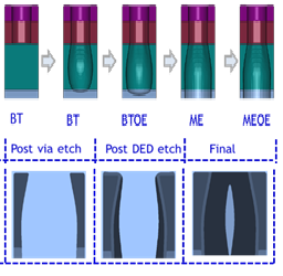
Figure 1: DED Process Calibration
In our 1st DOE, we performed a deposition and etch amount split experiment using the DED process steps. We learned that the void volume can be reduced but never eliminated under our test conditions, and that the deposition layer should not be greater than 45% of the top CD (see Fig.2).
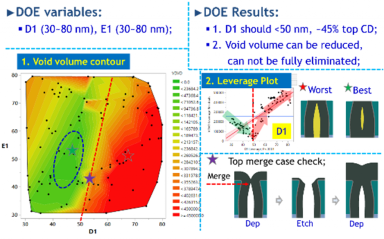
Figure 2: DED Contour, Level Plot, Output Structure of DOE1
Our second DOE added an additional deposition/etch process step to the calibrated model (a DEDED process sequence). These additional deposition & etch steps were set at the same deposition & etch ranges (D1 & E1) as were used in the first DOE. D1/E1 experimental splits demonstrated that a void free structure can be obtained at D1 & E1 values of 47 & 52 nm, respectively (see Fig. 3). Note that this DEDED process sequence has additional deposition and etch steps compared to DOE #1, which increases the process time and lowers the throughput compared to the simple DED process used earlier.
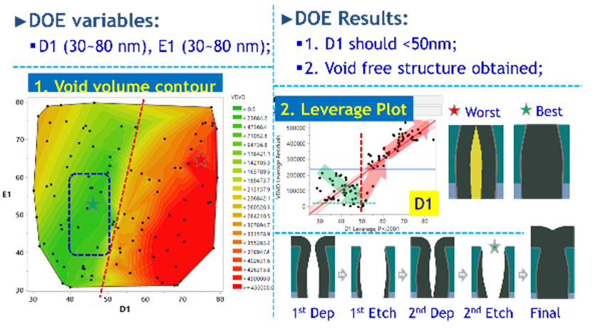
Figure 3: DEDED Contour, Level Plot and Output Structure of DOE2
In our 3rd DOE, we performed an incoming via profile split experiment by adjusting the BT etch behavior parameter. In the BT etch split, we used the visibility etch feature of SEMulator3D to model the process. The source sigma (BTA) and over etch factor (Fact) were the input parameters that we modified in the virtual experiment. After the virtual via etch was completed, virtual metrology was used to measure the maximum bow CD and location from each simulation run. Using this method, BTA (breakthrough source sigma) and Fact (over etch amount) experimental splits were used to generate virtual structures, and the bow cd and location were measured and plotted. Results from the 3rd DOE indicate that a void free structure can be obtained when the bow cd is small enough. We also learned that the void volume will dramatically increase when the bow cd >150 nm (see Fig. 4). With these results, we can now use the optimal 3rd DOE results to select our manufacturing parameters and proceed to Si validation.
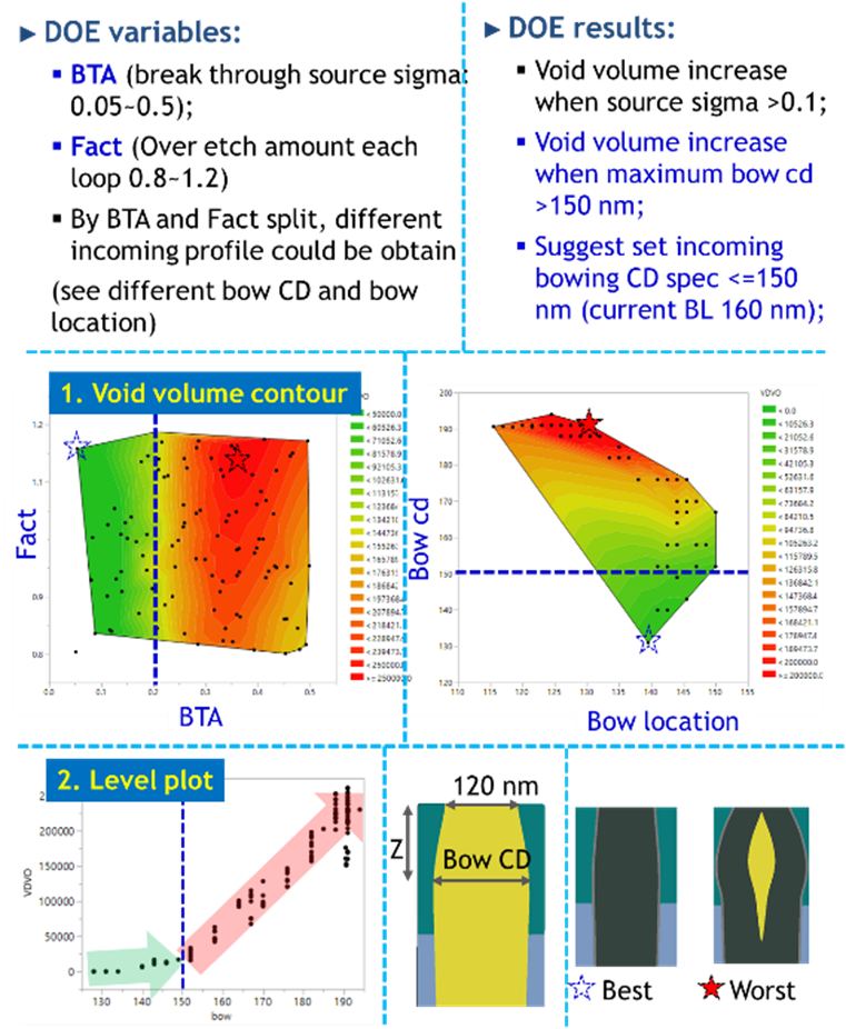
Figure 4: Incoming Via Profile Split Contour, Level Plot and Output Structure of DOE3
By setting our incoming via bowing spec <150 nm (145 nm in Figure 5), a void free structure was obtained in the final Si process. In this case, our silicon results matched our model prediction, and the void issue was solved.
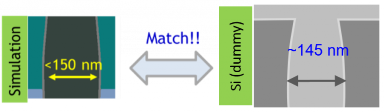
Figure 5. SEMulator3D Predicted Result and Actual Si results when the Bow CD <150 nm.
In this demonstration, SEMulator3D modeling and the execution of a virtual DOE were performed to optimize DED W filling and generate a void-free structure. A reduced void or void free structure was identified during all 3 of the DOEs. Si validation using the DOE3 results was completed, and demonstrated that we had solved the void issue. The Si result matched the model predictions, in a much shorter time than would be possible using trial and error validation. This experiment demonstrated that virtual DOEs can successfully reduce void volume in a DED W filling process, while accelerating process development and lowering Si wafer test costs.