At the beginning of my career in semiconductor equipment, the backside of the wafer was a source of anxiety. In one memorable instance in my early career, several wafers flew off a robot blade during a wafer transfer. After cleaning up the mess, we remembered that a variety of thin films could be deposited on the wafer backside, which could decrease its friction coefficient. Slowing down the wafer transfer helped to contain this issue, but we were left with unhappy business managers who had to explain the resulting reduction in throughput to customers.
Despite this rocky introduction to the wafer backside, I started paying more attention to the backside when the Xilinx Virtex-7 series of FPGAs was released in the early 2010’s. Xilinx’s products were some of the first FPGAs that used heterogeneous integration with “stacked silicon interconnect technology” [1]. This technology used a silicon interposer, which is used to route electrical signals or power between different FPGA components. The interposer is formed by creating TSVs (through silicon vias) partially through the silicon wafer and creating signal redistribution layers on top. The wafer backside is processed to connect both ends of the TSV’s: the frontside of the wafer is temporarily attached to a carrier wafer, and then the silicon interposer is processed upside down. Back grinding and etching are then used to expose the TSVs. By the time of Xilinx’s product introduction, I had left the industry to go back to graduate school. Metallization of TSV’s were a hot topic in class, and the backside of the wafer became a more interesting topic among engineers due to new developments in heterogeneous integration.
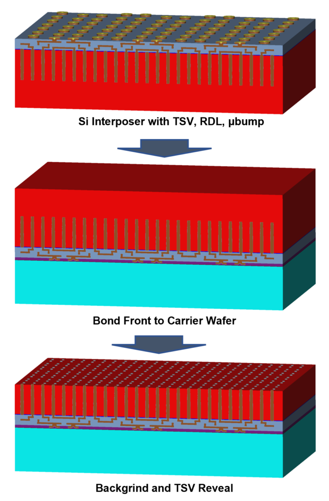
Figure 1. Silicon interposer processing. After vias and initial metallization, the backside of the wafer is ground down to reach the vias.
While a silicon interposer was used in the Xilinx FPGA to deal with signaling and bandwidth requirements, a more forward-looking approach is to remove the interposer and directly use the backside of the wafer for electrical routing. An example of “backside” architecture is backside power delivery, where the power supply is relocated from conventional BEOL on the front of the wafer to the backside. This architecture can potentially reduce the IR drop between the power rail and the active device. As an example of backside architecture, imec is pursuing the use of buried power rails at the fin level [2]. In imec’s process flow, the rails are constructed between fins and resemble a DRAM buried word line. BEOL is formed for signaling, and after completion, TSVs are created on the backside of the device wafer to provide access to the buried rails. Further interconnects can be added to the backside for power delivery.

Figure 2. Backside power delivery using buried power rails, based on [2] (not to scale).
The real estate on the backside of the device wafer certainly looks promising, at least for performance reasons. Moving the power rail from the front to the back side will enable cell scaling and limit the IR drop by reducing congestion on the front side of the wafer. The leading semiconductor logic companies are well aware of the benefits of backside power delivery, and are actively working to develop backside distribution networks. Intel announced in mid-2021 that they will use their “PowerVia” technology to implement backside power delivery, while TSMC has also discussed using Buried Power Rails in their next node technologies [3]. We look forward to seeing what’s next for the backside of the wafer.
References
- K. Saban. “Xilinx Stacked Silicon Interconnect Technology Delivers Breakthrough FPGA Capacity, Bandwidth, and Power Efficiency”, Xilinx WP380, 2012.
- J. Ryckaert et al., “Extending the roadmap beyond 3nm through system scaling boosters: A case study on Buried Power Rail and Backside Power Delivery,” 2019 Electron Devices Technology and Manufacturing Conference (EDTM), 2019, pp. 50-52, doi: 10.1109/EDTM.2019.8731234.
- D. O’Laughlin, “Backside Power Delivery and Bold Bets at Intel”, https://www.fabricatedknowledge.com/p/backside-power-delivery-and-bold