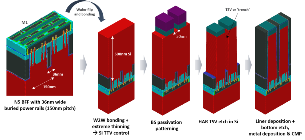
Backside Power Delivery as a Scaling Knob for Future Systems
July 3, 2019
Speeding Up Process Optimization with Virtual Processing
November 6, 2019You must have an account on our Customer Portal to access this content. If you already have an account, please log in using the form below or to the right. If you do not have an account, we invite you to request an account.
Whitepaper: Advances in 3D CMOS Image Sensors Optical Modeling: Combining Realistic Morphologies with FDTD
To download your free white paper, please fill out the form below:
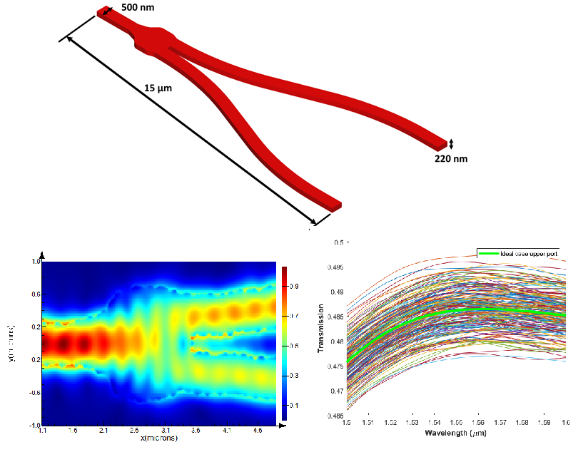
This paper describes an innovative methodology to investigate the relationship between device morphology and the optical performance of CMOS image sensors. By coupling a FDTD-based 3D Maxwell solver with silicon-accurate process modeling software, we have been able to analyze the sensitivity of image sensor quantum efficiency with respect to statistical variations in nm-scale device topology.
© 2019 IEEE. Personal use of this material is permitted. Permission from IEEE must be obtained for all other uses, in any current or future media, including reprinting/republishing this material for advertising or promotional purposes, creating new collective works, for resale or redistribution to servers or lists, or reuse of any copyrighted component of this work in other works.
You might also be interested in:
- You must have an account on our Customer Portal to access this content. If you already have an account, please log in using the form below or to the right. […]