Skip to main content
LOG IN
REGISTER
Home
Customer Portal
Coventor Licensing Downloads
SEMulator3D Downloads
CoventorMP Downloads
Webinars
MEMS+ Courses
System Requirements
Software Licensing
Contact Us
✕
Enter your search
(more…)
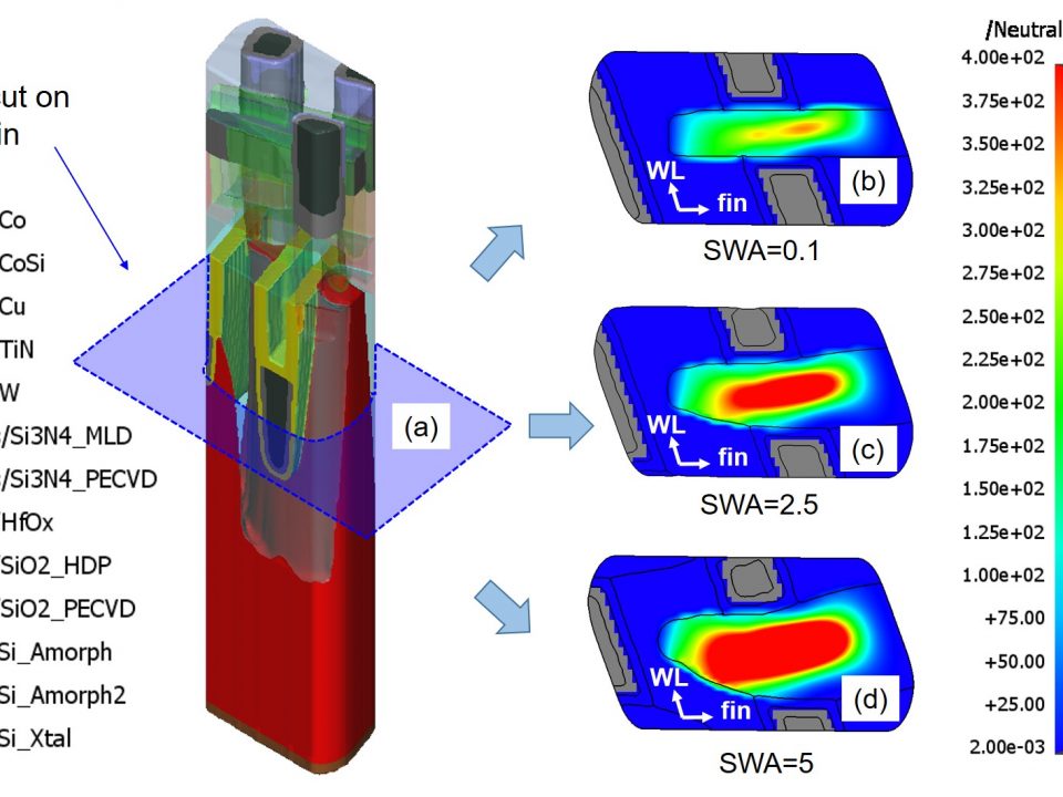
A Study of Wiggling AA Modeling and its Impact on Device Performance in Advanced DRAM
Read more
- A Study of Wiggling AA Modeling and its Impact on Device Performance in Advanced DRAM
A Study of Wiggling AA Modeling and its Impact on Device Performance in Advanced DRAM
(more…)
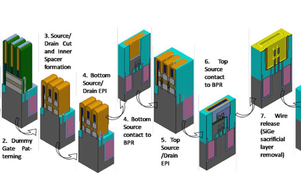
A Benchmark Study of Complementary-Field Effect Transistor (CFET) Process Integration Options: Comparing Bulk vs. SOI vs. DSOI Starting Substrates
Read more
- A Benchmark Study of Complementary-Field Effect Transistor (CFET) Process Integration Options: Comparing Bulk vs. SOI vs. DSOI Starting Substrates
A Benchmark Study of Complementary-Field Effect Transistor (CFET) Process Integration Options: Comparing Bulk vs. SOI vs. DSOI Starting Substrates
(more…)
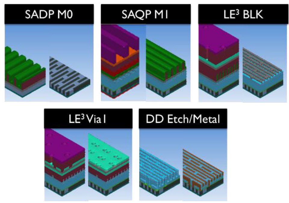
A million wafer, virtual fabrication approach to determine process capability requirements for an industry-standard N5 BEOL two-level metal flow
Read more
- A million wafer, virtual fabrication approach to determine process capability requirements for an industry-standard N5 BEOL two-level metal flow
A million wafer, virtual fabrication approach to determine process capability requirements for an industry-standard N5 BEOL two-level metal flow
(more…)
Defect Evolution in Next Generation, Extreme Ultraviolet Lithography
Read more
- Defect Evolution in Next Generation, Extreme Ultraviolet Lithography
Defect Evolution in Next Generation, Extreme Ultraviolet Lithography
(more…)
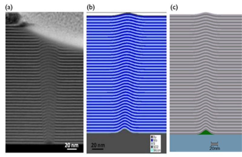
3D NAND Flash Processing
Read more
- 3D NAND Flash Processing
3D NAND Flash Processing
(more…)
Contact Us
LOG IN
REGISTER
![3D NAND flash memory array, based on TCAT [1], with 16 cells per string, top gate-select layer and bottom source-select layer.](https://www.coventor.com/wp-content/uploads/2014/05/TCAT_whole_bf-M1-marked1.png)