Speeding Up Process Optimization with Virtual Processing
November 6, 2019
Impact of EUV Resist Thickness on Local Critical Dimension Uniformities for <30 nm CD Via Patterning
March 30, 2020You must have an account on our Customer Portal to access this content. If you already have an account, please log in using the form below or to the right. If you do not have an account, we invite you to request an account.
Whitepaper: A Benchmark Study of Complementary-Field Effect Transistor (CFET) Process Integration Options: Comparing Bulk vs. SOI vs. DSOI Starting Substrates

To download your free white paper, please fill out the form below:
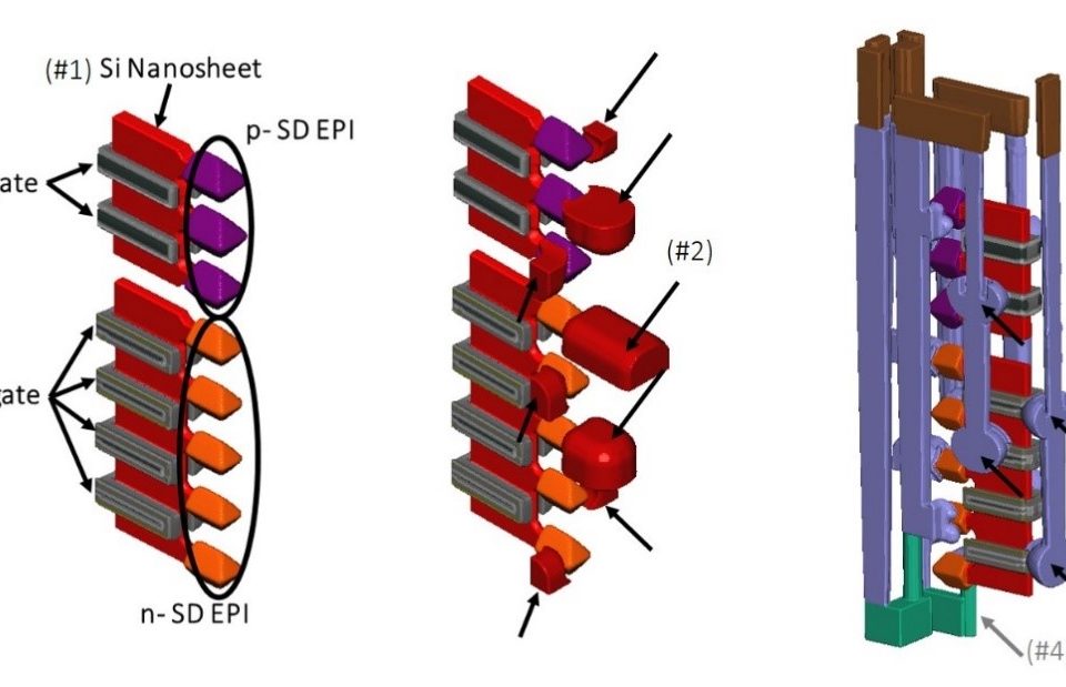
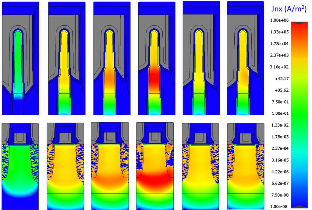
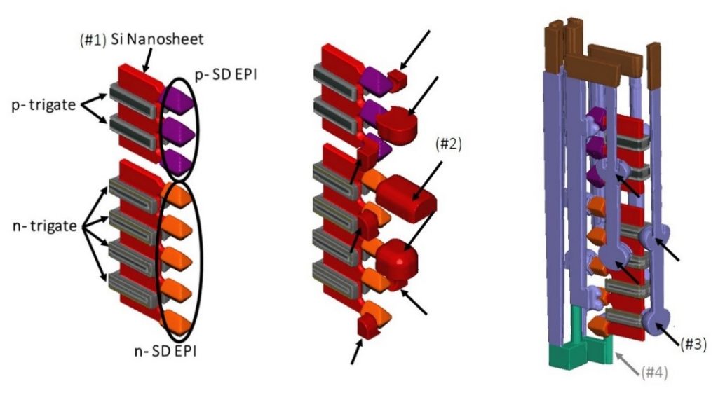
Sub-5 nm logic nodes will require an extremely high level of innovation to overcome the inherent real-estate limitations at this increased device density. One approach to increasing device density is to look at the vertical device dimension (z-direction), and stack devices on top of each other instead of conventionally side-by-side. The fabrication of a Complementary-Field Effect Transistor (CFET) technology can be accomplished by directly fabricating n-MOS transistors on top of p-MOS transistors or vice-versa. This architecture will require new metal wiring designs and Buried Power Rails (BPR) within the substrate. The design will be disruptive and will require the development of specific new processing steps such as dielectric selective deposition on metal. In this study, we have used Coventor’s SEMulator3D platform with 3 CFET reference designs/process flows to understand design-process interaction risk in advance of any first mask tape-out and/or first wafer start. Each process flow that was compared had a specific Si starting substrate type: bulk, Silicon-On-Insulator (SOI), and Double Silicon-On-Insulator (DSOI). We compare the 3 process flows in terms of their robustness to process variation and identify the one with the lowest likelihood of processing failures.
© 2019 IEEE. Personal use of this material is permitted. Permission from IEEE must be obtained for all other uses, in any current or future media, including reprinting/republishing this material for advertising or promotional purposes, creating new collective works, for resale or redistribution to servers or lists, or reuse of any copyrighted component of this work in other works.
You might also be interested in:
- You must have an account on our Customer Portal to access this content. If you already have an account, please log in using the form below or to the right. […]
- You must have an account on our Customer Portal to access this content. If you already have an account, please log in using the form below or to the right. […]
- You must have an account on our Customer Portal to access this content. If you already have an account, please log in using the form below or to the right. […]
- You must have an account on our Customer Portal to access this content. If you already have an account, please log in using the form below or to the right. […]
- You must have an account on our Customer Portal to access this content. If you already have an account, please log in using the form below or to the right. […]
- You must have an account on our Customer Portal to access this content. If you already have an account, please log in using the form below or to the right. […]


