Evaluating MEMS Device Virtual Metrology & DRIE
March 18, 2014
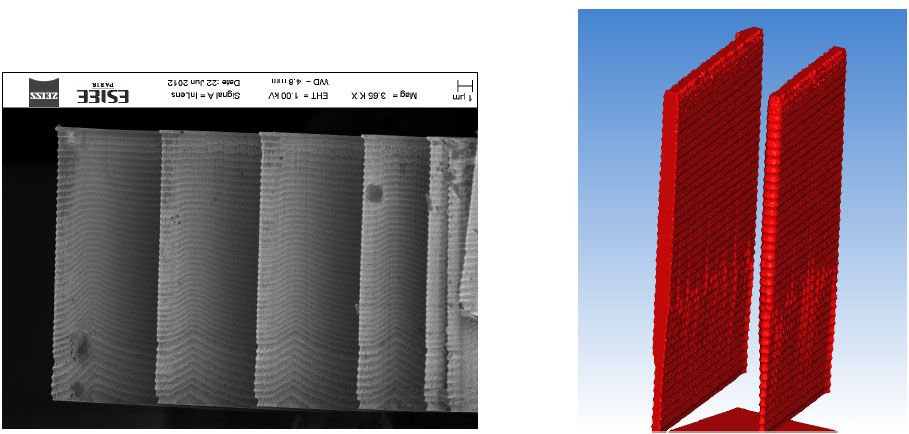
Modeling of Cross Wafer Induced Process Variations
October 6, 2015You must have an account on our Customer Portal to access this content. If you already have an account, please log in using the form below or to the right. If you do not have an account, we invite you to request an account.
Whitepaper: 3D NAND Flash Processing

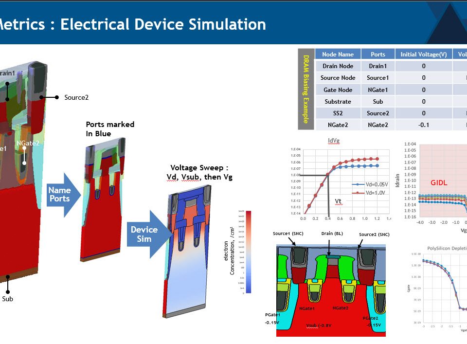
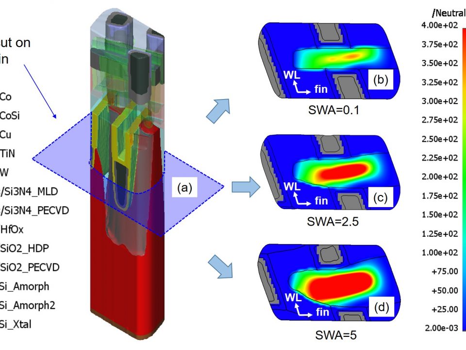
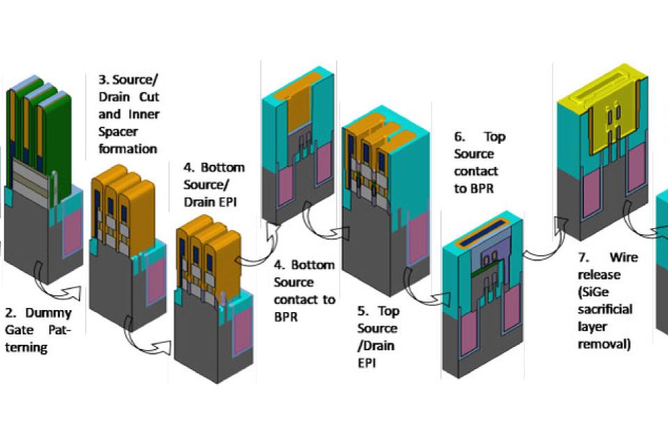
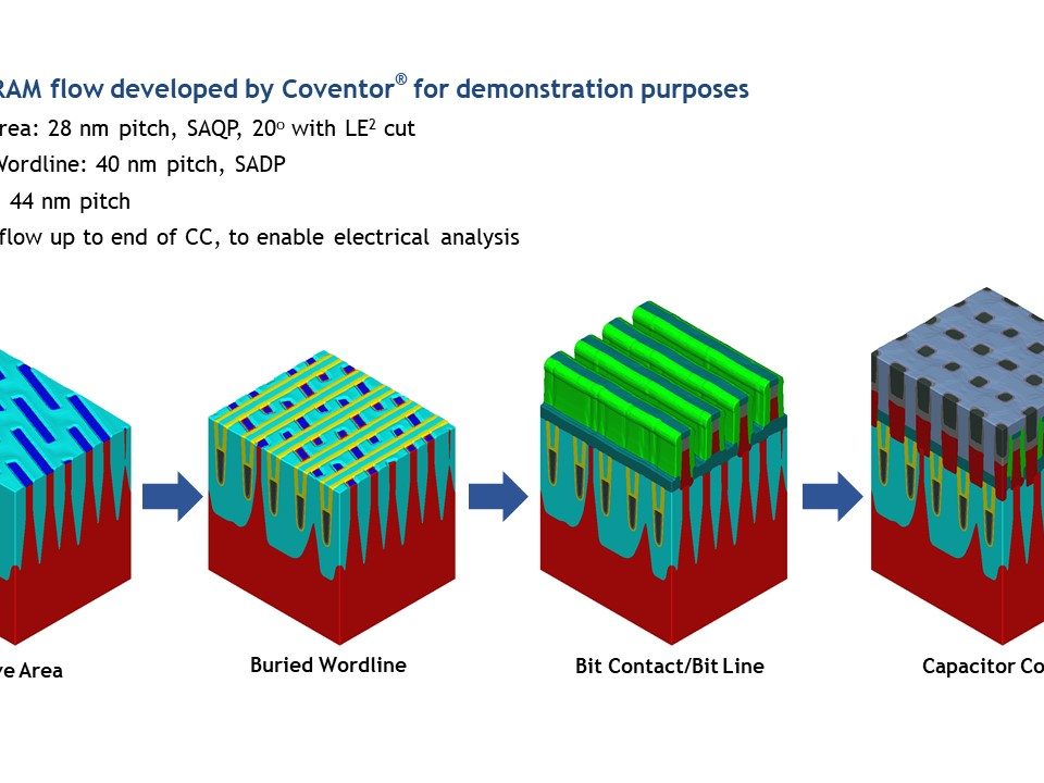
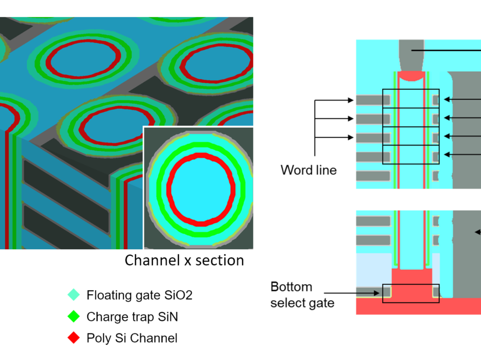
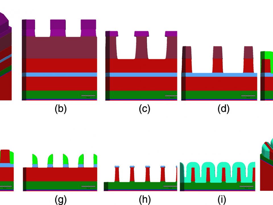
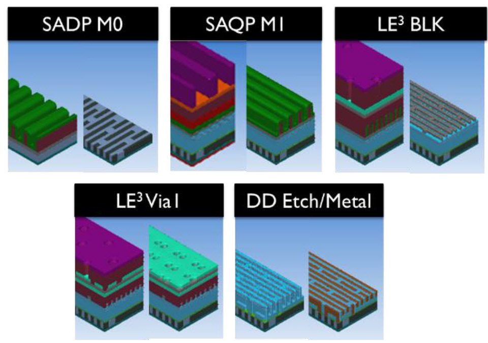
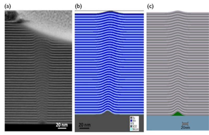
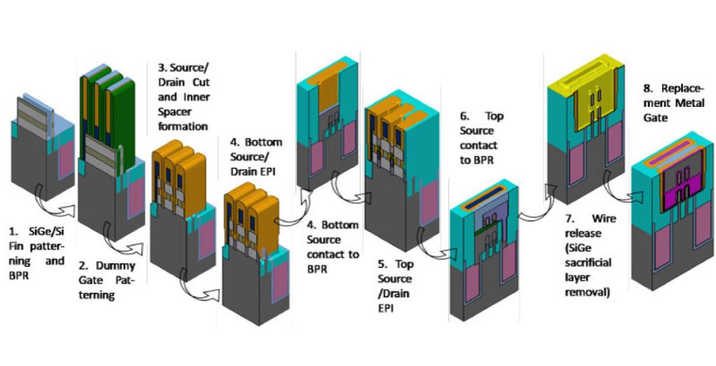
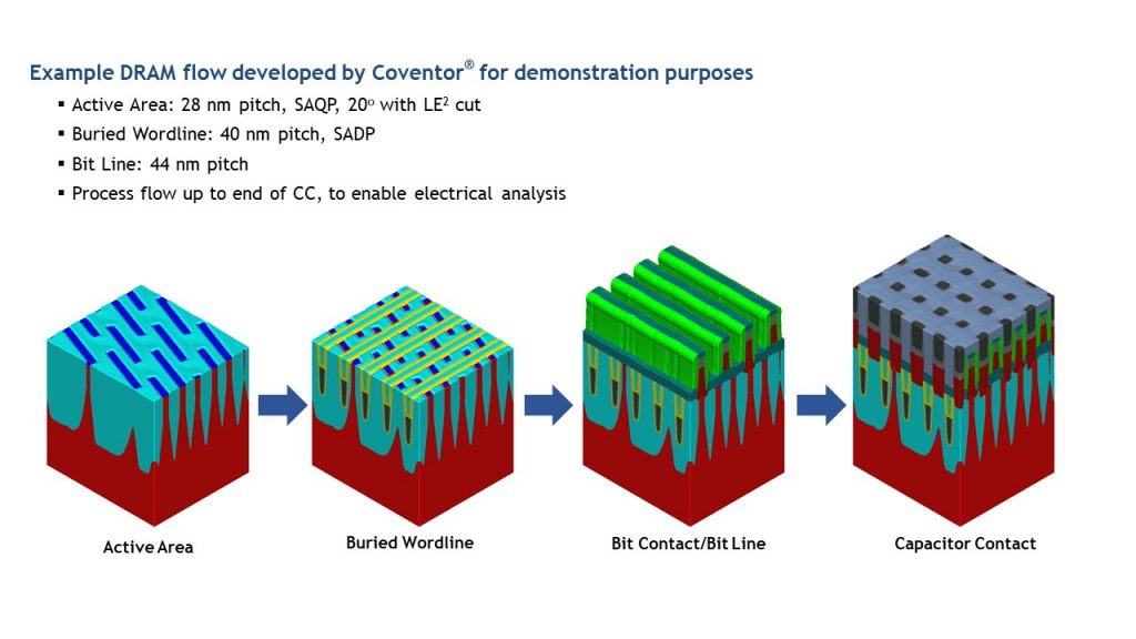
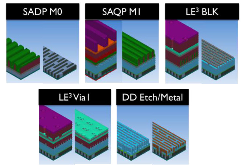
Coventor’s powerful SEMulator3D semiconductor process modeling platform offers a wide range of technology development capabilities for the development of cutting edge 3D NAND Flash Technology. 3D NAND promises high memory cell density with reduced data corruption, but also brings processing challenges. The structural complexity and inherent 3D nature of devices using 3D NAND require a predictive 3D modeling platform to perform critical analysis. The interactions between different modules and understanding defect evolution in such structures have become increasingly difficult. SEMulator3D is optimally suited for this work, due to its industry-leading predictive modeling performance and accuracy. This paper reviews how using virtual fabrication techniques with SEMulator3D, issues in 3D NAND Flash can be anticipated early, reducing development time and saving silicon runs.
You might also be interested in:
- You must have an account on our Customer Portal to access this content. If you already have an account, please log in using the form below or to the right. […]
- You must have an account on our Customer Portal to access this content. If you already have an account, please log in using the form below or to the right. […]
- You must have an account on our Customer Portal to access this content. If you already have an account, please log in using the form below or to the right. […]
- You must have an account on our Customer Portal to access this content. If you already have an account, please log in using the form below or to the right. […]
- You must have an account on our Customer Portal to access this content. If you already have an account, please log in using the form below or to the right. […]
- You must have an account on our Customer Portal to access this content. If you already have an account, please log in using the form below or to the right. […]
- You must have an account on our Customer Portal to access this content. If you already have an account, please log in using the form below or to the right. […]
- You must have an account on our Customer Portal to access this content. If you already have an account, please log in using the form below or to the right. […]
- You must have an account on our Customer Portal to access this content. If you already have an account, please log in using the form below or to the right. […]
