Self-aligned quadruple patterning to meet requirements for fins with high density
May 20, 2016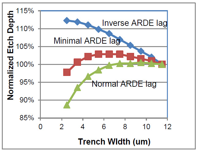
New Techniques to Analyze and Reduce Etch Variation
January 20, 2017You must have an account on our Customer Portal to access this content. If you already have an account, please log in using the form below or to the right. If you do not have an account, we invite you to request an account.
Whitepaper: A million wafer, virtual fabrication approach to determine process capability requirements for an industry-standard N5 BEOL two-level metal flow
To download your free white paper, please fill out the form below:
Process simulation can provide vital insights into identifying key process steps where wafer resources can be dedicated to improve yield or where investments should be made in tool capability. We considered this problem in the context of an industry-like N5 BEOL flow being developed at imec, and modeled the ~150 step N5 BEOL flow in Coventor SEMulator3D®. For the first time, a 1 million wafer DOE was conducted to sample a 10 dimensional variable space and derive the failure points for each process parameter. A vector based algorithm was used to search the parameter space and derive a hyper-surface to represent the absolute yield limits. The virtual wafers were generated to identify process sensitivities and spec limits for expected process variations. This work highlights that process optimization is needed to improve the capability of processes as they approach 1nm in feature size. This methodology could be useful in screening standard libraries for process sensitivities.
You might also be interested in:
- You must have an account on our Customer Portal to access this content. If you already have an account, please log in using the form below or to the right. […]
- You must have an account on our Customer Portal to access this content. If you already have an account, please log in using the form below or to the right. […]
- You must have an account on our Customer Portal to access this content. If you already have an account, please log in using the form below or to the right. […]
- You must have an account on our Customer Portal to access this content. If you already have an account, please log in using the form below or to the right. […]
- You must have an account on our Customer Portal to access this content. If you already have an account, please log in using the form below or to the right. […]
- You must have an account on our Customer Portal to access this content. If you already have an account, please log in using the form below or to the right. […]


