Skip to main content
LOG IN
REGISTER
Home
Customer Portal
Coventor Licensing Downloads
SEMulator3D Downloads
CoventorMP Downloads
Webinars
MEMS+ Courses
System Requirements
Software Licensing
Contact Us
✕
Enter your search
(more…)
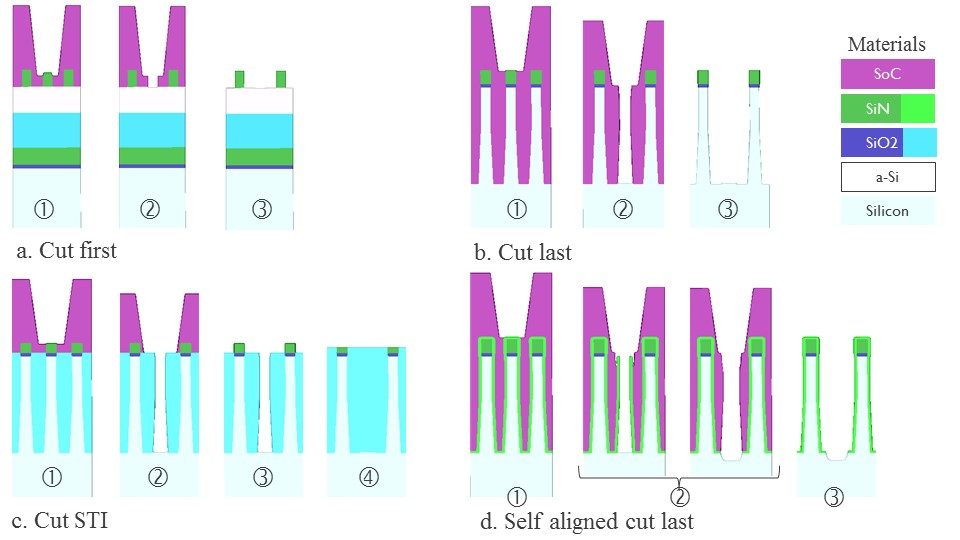
Self-aligned Fin Cut Last Patterning Scheme for Fin Arrays of 24nm Pitch and Beyond
Read more
- Self-aligned Fin Cut Last Patterning Scheme for Fin Arrays of 24nm Pitch and Beyond
Self-aligned Fin Cut Last Patterning Scheme for Fin Arrays of 24nm Pitch and Beyond
(more…)
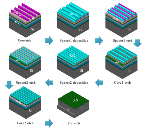
N7 FinFET Self-Aligned Quadruple Patterning Modeling
Read more
- N7 FinFET Self-Aligned Quadruple Patterning Modeling
N7 FinFET Self-Aligned Quadruple Patterning Modeling
(more…)
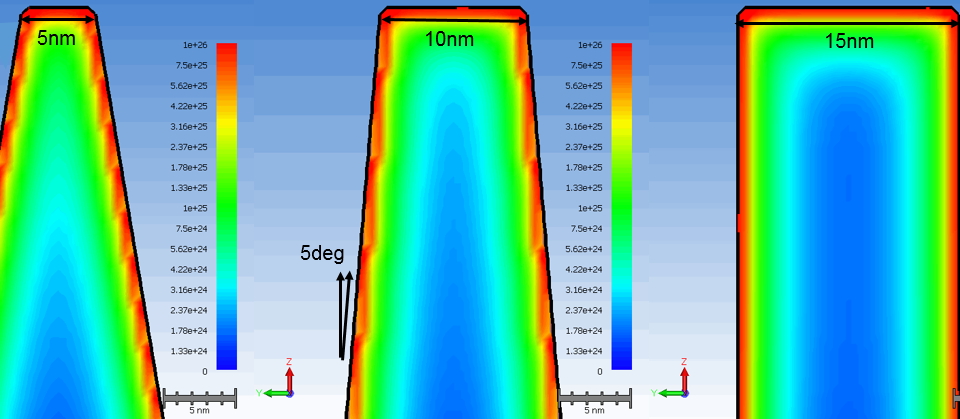
Understanding the Effect of Variability in Bulk FinFET Device Performance
Read more
- Understanding the Effect of Variability in Bulk FinFET Device Performance
Understanding the Effect of Variability in Bulk FinFET Device Performance
(more…)
Understanding how small variations in photoresist shape significantly impact multi-patterning yield
Read more
- Understanding how small variations in photoresist shape significantly impact multi-patterning yield
Understanding how small variations in photoresist shape significantly impact multi-patterning yield
(more…)
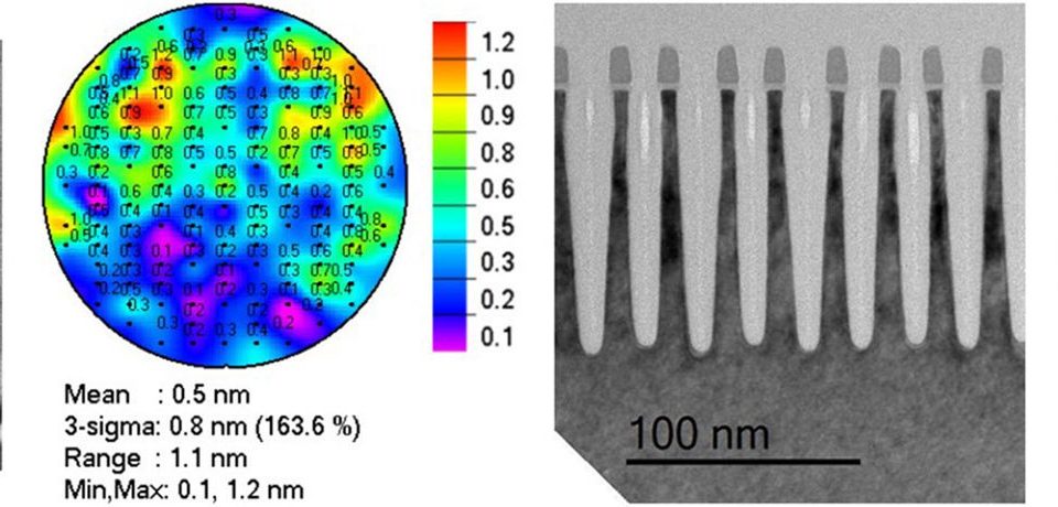
Self-aligned quadruple patterning to meet requirements for fins with high density
Read more
- Self-aligned quadruple patterning to meet requirements for fins with high density
Self-aligned quadruple patterning to meet requirements for fins with high density
(more…)
Modeling of Cross Wafer Induced Process Variations
Read more
- Modeling of Cross Wafer Induced Process Variations
Modeling of Cross Wafer Induced Process Variations
(more…)
FinFET Front End of Line FEOL Process Integration
Read more
- FinFET Front End of Line FEOL Process Integration
FinFET Front End of Line FEOL Process Integration
(more…)
Contact Us
LOG IN
REGISTER
