Defect Evolution in Next Generation, Extreme Ultraviolet Lithography
February 20, 2016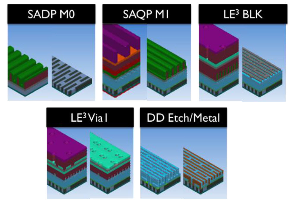
A million wafer, virtual fabrication approach to determine process capability requirements for an industry-standard N5 BEOL two-level metal flow
December 1, 2016You must have an account on our Customer Portal to access this content. If you already have an account, please log in using the form below or to the right. If you do not have an account, we invite you to request an account.
Whitepaper: Self-aligned quadruple patterning to meet requirements for fins with high density
To download your free white paper, please fill out the form below:
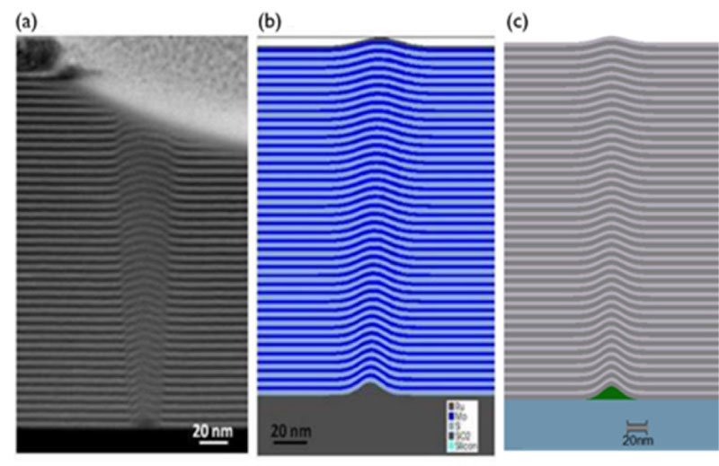
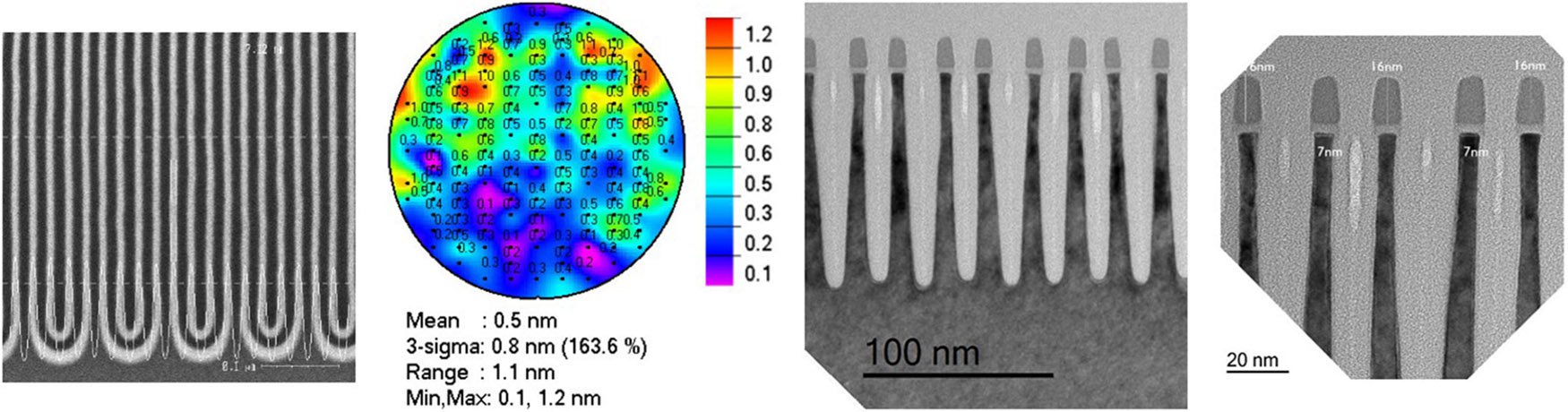
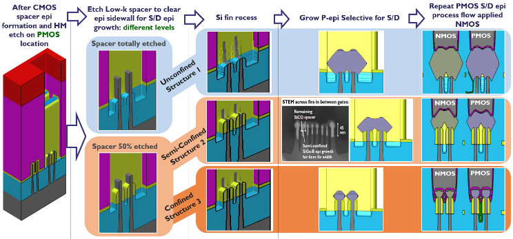
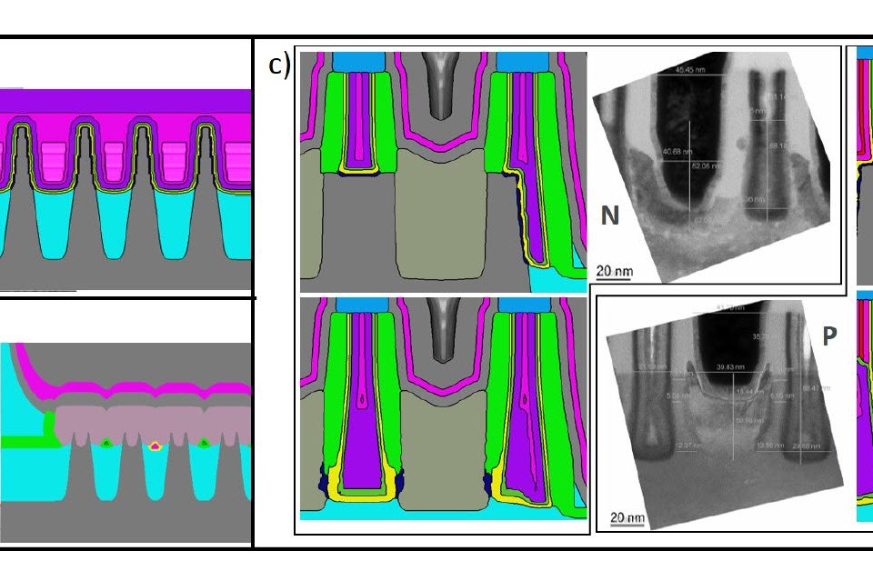
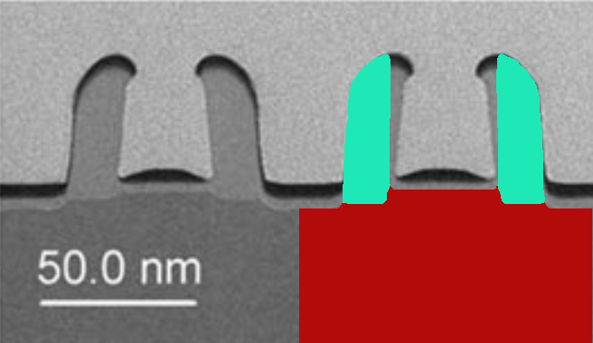
Over recent decades, continuous reductions in the scale of field-effect transistors in accordance with Moore's law, which states that the number of transistors in an integrated circuit doubles every two years, have enabled continuous increases in device performance and transistor density.1–3 Currently, state-of-the-art devices are based on structural elements with dimensions of 7nm or even 5nm (N7/N5). The highest-resolution patterns required for N7/N5 devices are silicon fins with a pitch of 18–28nm and metal layers with a pitch of 24–32nm. These dimensions far exceed the resolution attainable with 193 immersion (193i) lithography. Extreme UV lithography might be an alternative process for the formation of lines and spaces, but is expensive and not entirely ready for use in production. To overcome the limitations of lithography, multiple patterning methods—litho-etch or self-aligned multiple patterning—were used in the last four stages of device miniaturization based on nodes of 10–28nm (N10–N28).5, 6 To achieve the specifications for fins in N7/N5 devices, we need a self-aligned quadruple patterning (SAQP) method that provides a critical dimension (CD) of about 7nm, a CD uniformity (CDU) and pitch walk of 0.5nm (3 sigma), and a line width roughness (LWR) and line edge roughness (LER) of 1.4 and 1.2nm, respectively.
You might also be interested in:
- You must have an account on our Customer Portal to access this content. If you already have an account, please log in using the form below or to the right. […]
- You must have an account on our Customer Portal to access this content. If you already have an account, please log in using the form below or to the right. […]
- You must have an account on our Customer Portal to access this content. If you already have an account, please log in using the form below or to the right. […]
- You must have an account on our Customer Portal to access this content. If you already have an account, please log in using the form below or to the right. […]
- You must have an account on our Customer Portal to access this content. If you already have an account, please log in using the form below or to the right. […]
- You must have an account on our Customer Portal to access this content. If you already have an account, please log in using the form below or to the right. […]

