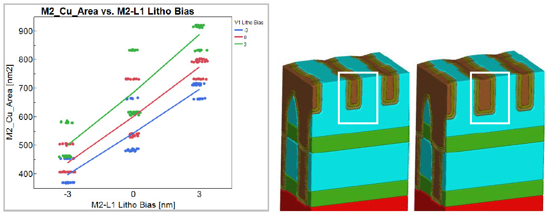
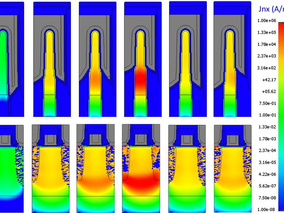
Back-End-of-Line (BEOL) Virtual Patterning
May 26, 2013You must have an account on our Customer Portal to access this content. If you already have an account, please log in using the form below or to the right. If you do not have an account, we invite you to request an account.
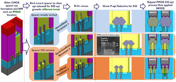
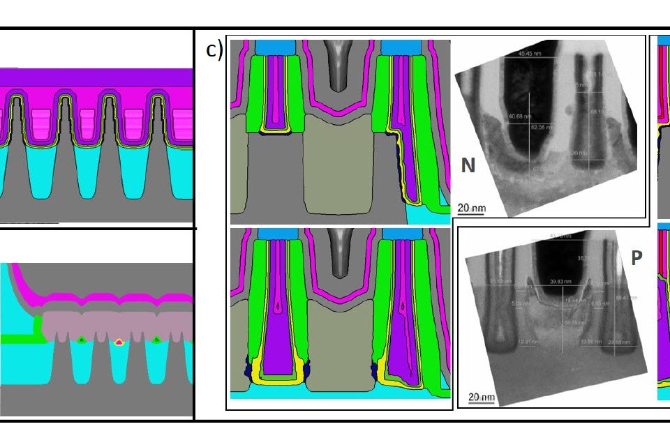
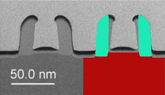
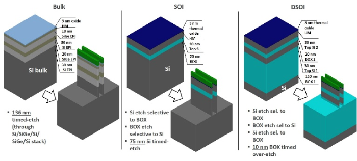
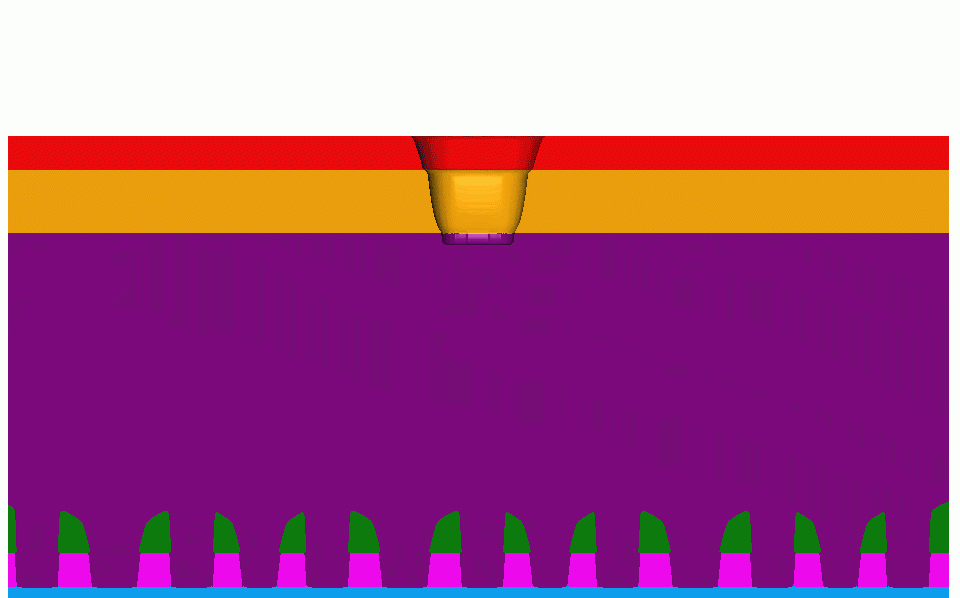
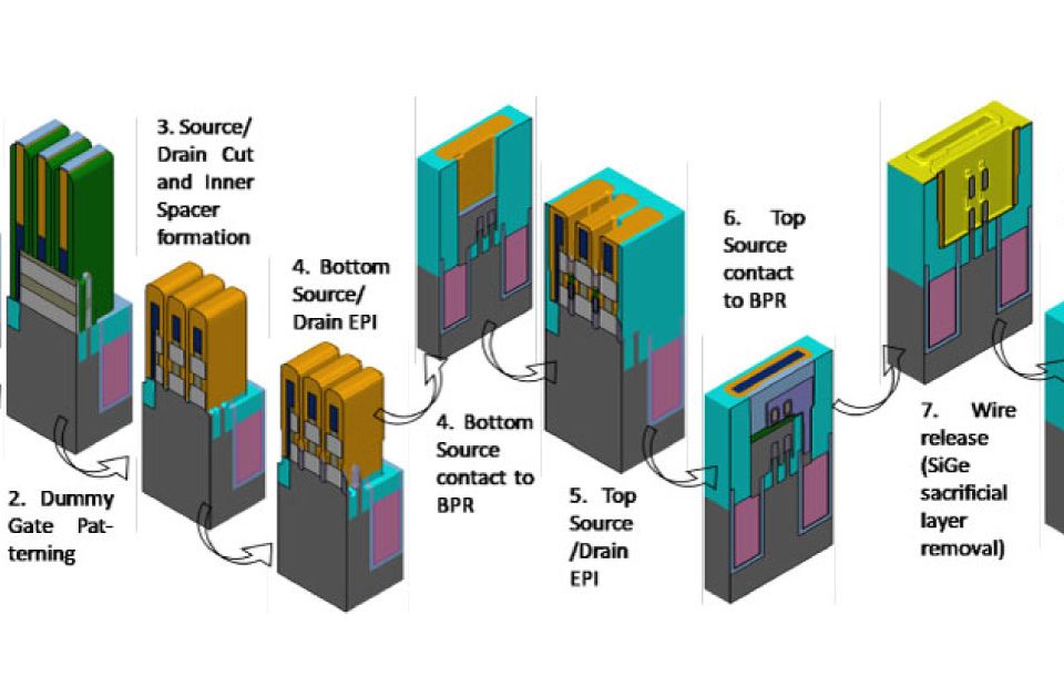
Whitepaper: FinFET Front End of Line FEOL Process Integration

Purely geometric scaling of transistors ended around the 90-nanometer (nm) era. Since then, most power/performance and area/cost improvements have come from structural and material innovations. Silicon-on-Insulator (SOI), first “partially depleted” and more recently “fully depleted” as well as embedded stressors, High-K / Metal-Gate (HKMG) and now FinFETs are examples of technology innovations that have been required to continue scaling below 90nm. Virtual fabrication with Coventor’s SEMulator3D process modeling platform offers capabilities that reduce the time and resources required to develop advanced technologies through predictive design technology modeling, variation analysis and quantitative data extraction. This white paper demonstrates virtual fabrication capabilities through examples in the development of a hypothetical FinFET technology.
You might also be interested in:
- You must have an account on our Customer Portal to access this content. If you already have an account, please log in using the form below or to the right. […]
- You must have an account on our Customer Portal to access this content. If you already have an account, please log in using the form below or to the right. […]
- You must have an account on our Customer Portal to access this content. If you already have an account, please log in using the form below or to the right. […]
- You must have an account on our Customer Portal to access this content. If you already have an account, please log in using the form below or to the right. […]
- You must have an account on our Customer Portal to access this content. If you already have an account, please log in using the form below or to the right. […]
- You must have an account on our Customer Portal to access this content. If you already have an account, please log in using the form below or to the right. […]
- You must have an account on our Customer Portal to access this content. If you already have an account, please log in using the form below or to the right. […]
Impact of EUV Resist Thickness on Local Critical Dimension Uniformities for <30 nm CD Via Patterning
Impact of EUV Resist Thickness on Local Critical Dimension Uniformities for <30 nm CD Via Patterning
You must have an account on our Customer Portal to access this content. If you already have an account, please log in using the form below or to the right. […]- You must have an account on our Customer Portal to access this content. If you already have an account, please log in using the form below or to the right. […]
- You must have an account on our Customer Portal to access this content. If you already have an account, please log in using the form below or to the right. […]
- You must have an account on our Customer Portal to access this content. If you already have an account, please log in using the form below or to the right. […]
- You must have an account on our Customer Portal to access this content. If you already have an account, please log in using the form below or to the right. […]

