Skip to main content
LOG IN
REGISTER
Home
Customer Portal
Coventor Licensing Downloads
SEMulator3D Downloads
CoventorMP Downloads
Webinars
MEMS+ Courses
System Requirements
Software Licensing
Contact Us
✕
Enter your search
(more…)
The Effects of Poly Corner Etch Residue on Advanced FinFET Device Performance
Read more
- The Effects of Poly Corner Etch Residue on Advanced FinFET Device Performance
The Effects of Poly Corner Etch Residue on Advanced FinFET Device Performance
(more…)
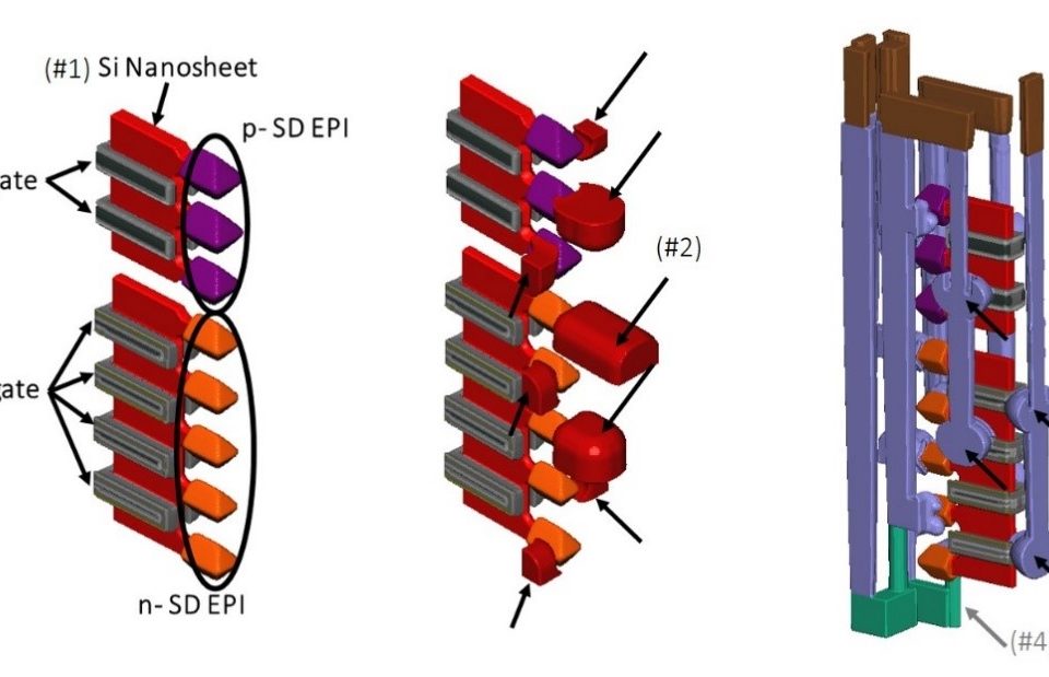
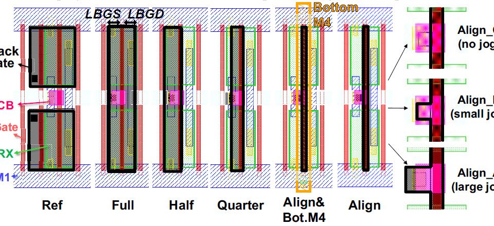
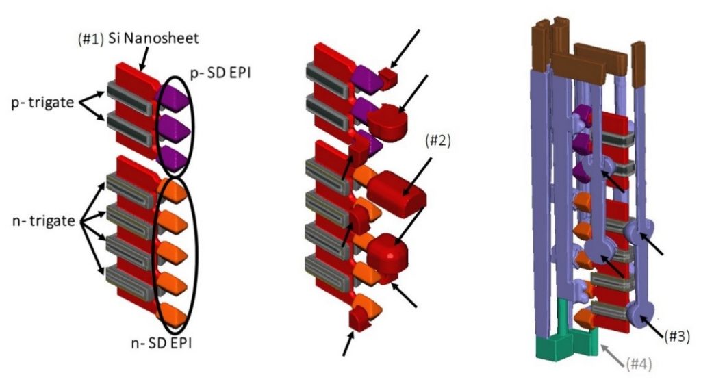
SVT (six stacked vertical transistors) SRAM cell architecture introduction: design and process challenges assessment
Read more
- SVT (six stacked vertical transistors) SRAM cell architecture introduction: design and process challenges assessment
SVT (six stacked vertical transistors) SRAM cell architecture introduction: design and process challenges assessment
(more…)
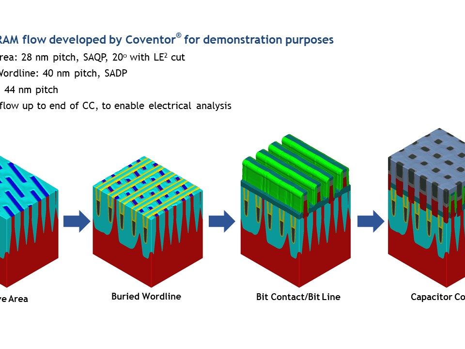
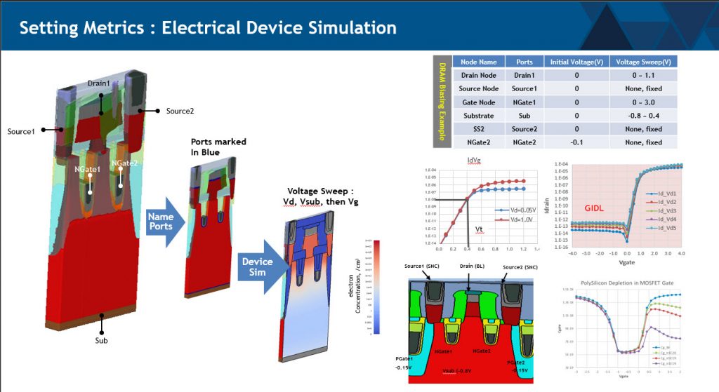
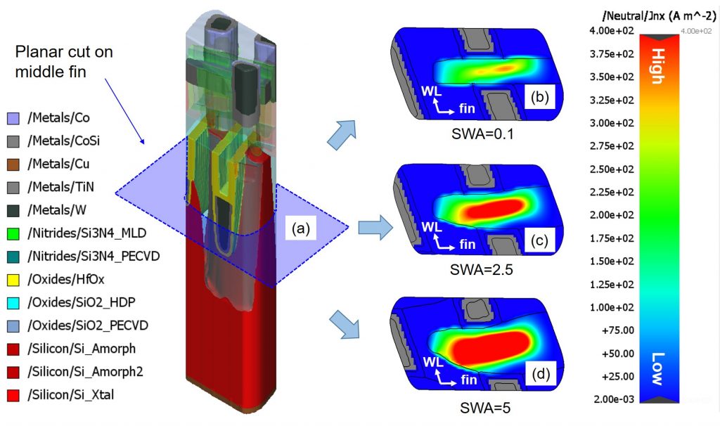
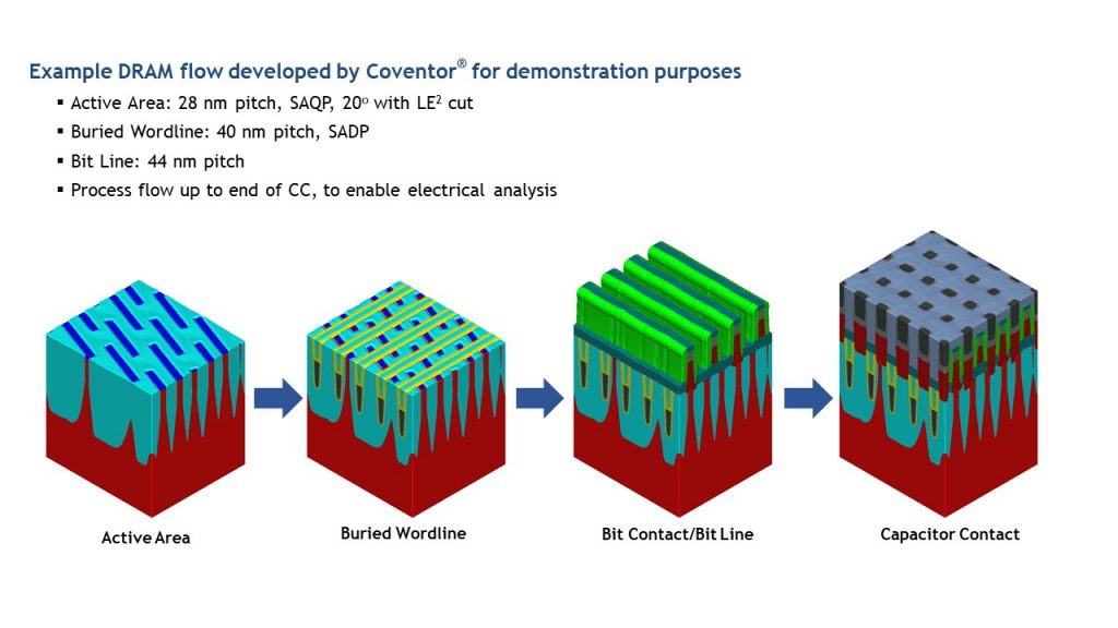
Process Window Optimization of DRAM by Virtual Fabrication
Read more
- Process Window Optimization of DRAM by Virtual Fabrication
Process Window Optimization of DRAM by Virtual Fabrication
(more…)
A Study of Wiggling AA Modeling and its Impact on Device Performance in Advanced DRAM
Read more
- A Study of Wiggling AA Modeling and its Impact on Device Performance in Advanced DRAM
A Study of Wiggling AA Modeling and its Impact on Device Performance in Advanced DRAM
(more…)
Speeding Up Process Optimization with Virtual Processing
Read more
- Speeding Up Process Optimization with Virtual Processing
Speeding Up Process Optimization with Virtual Processing
(more…)
Design Technology Co-Optimization of 3D-monolithic standard cells and SRAM exploiting dynamic back-bias for ultra-low-voltage operation
Read more
- Design Technology Co-Optimization of 3D-monolithic standard cells and SRAM exploiting dynamic back-bias for ultra-low-voltage operation
Design Technology Co-Optimization of 3D-monolithic standard cells and SRAM exploiting dynamic back-bias for ultra-low-voltage operation
(more…)
Contact Us
LOG IN
REGISTER
