
A Triple-Deck CFET Structure with an Integrated SRAM Cell for the 2nm Technology Node and Beyond
January 19, 2021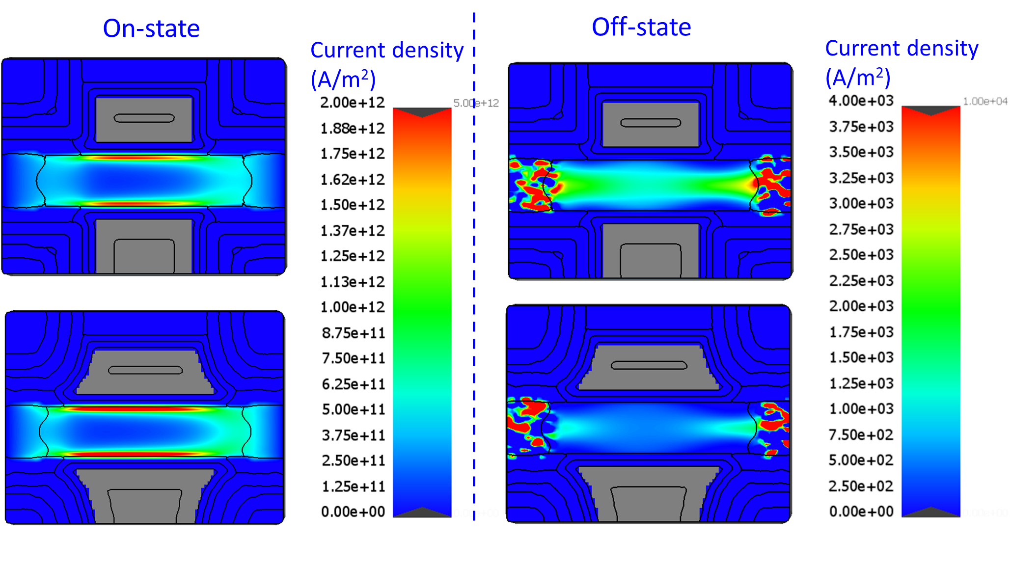
The Effects of Poly Corner Etch Residue on Advanced FinFET Device Performance
June 16, 2021You must have an account on our Customer Portal to access this content. If you already have an account, please log in using the form below or to the right. If you do not have an account, we invite you to request an account.
Whitepaper: SVT (six stacked vertical transistors) SRAM cell architecture introduction: design and process challenges assessment

To download your free white paper, please fill out the form below:
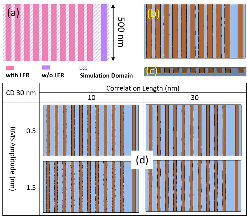
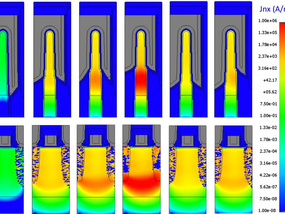
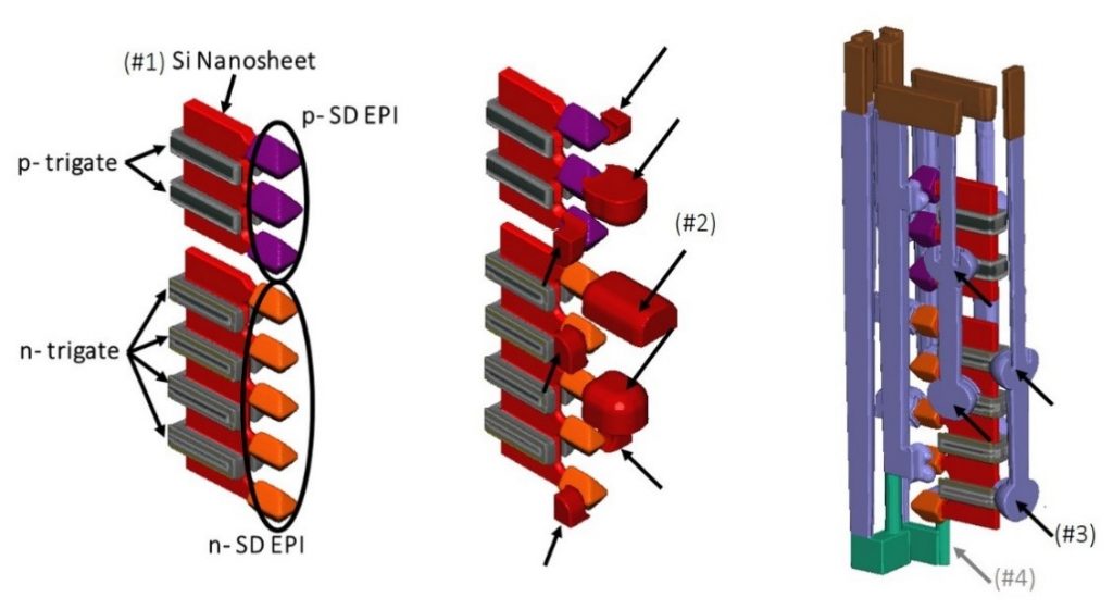
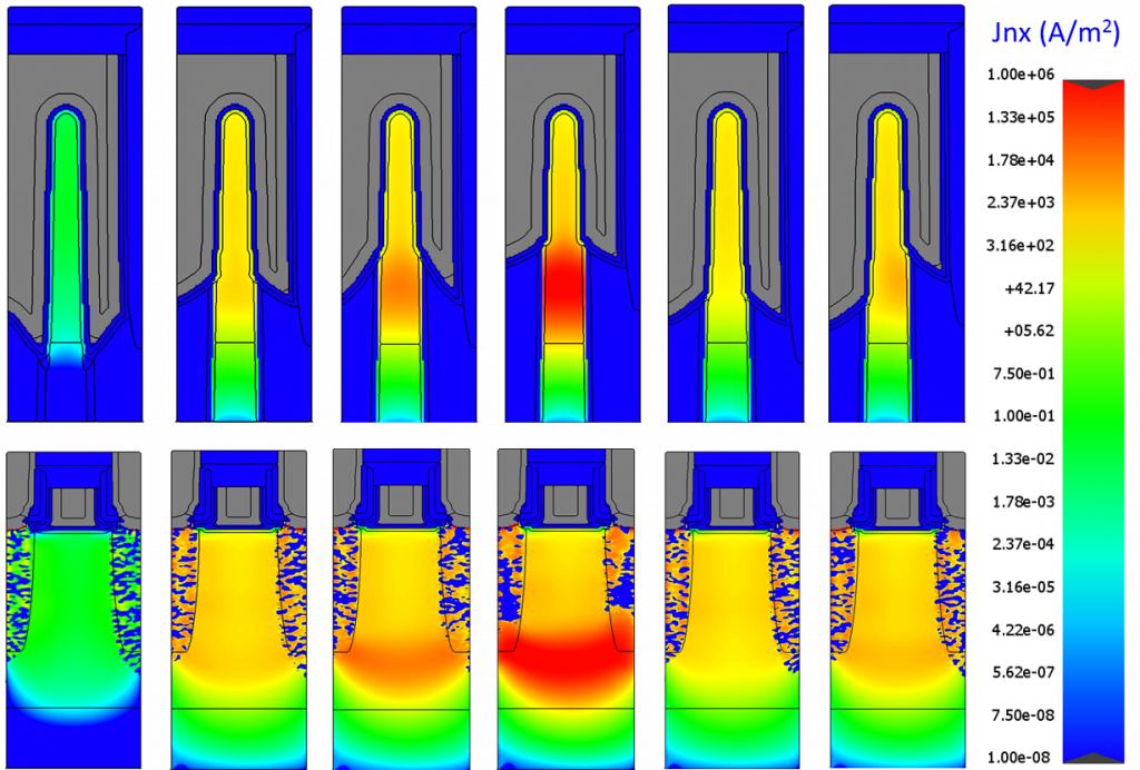
This paper presents a new design architecture for advanced logic SRAM cells using six vertical transistors (with carrier transport along the Z direction), stacked one on top of each other. Virtual fabrication technology was used to identify different process integration schemes to enable the fabrication of this architecture with a competitive XY footprint at an advanced logic node: a unit cell area of 0.0093 um2 was demonstrated in this work. This study illustrates that virtual fabrication can be a key enabling element for technology pathfinding, and that it can be used to identify expected module development challenges prior to tape-out or wafer processing.
B. Vincent, J. Ervin, "SSVT (six stacked vertical transistors) SRAM cell architecture introduction: design and process challenges assessment," Proc. SPIE 11614, Design-Process-Technology Co-optimization XV, 116140E (22 February 2021); doi: 10.1117/12.2583414
You might also be interested in:
- You must have an account on our Customer Portal to access this content. If you already have an account, please log in using the form below or to the right. […]
- You must have an account on our Customer Portal to access this content. If you already have an account, please log in using the form below or to the right. […]
- You must have an account on our Customer Portal to access this content. If you already have an account, please log in using the form below or to the right. […]
- You must have an account on our Customer Portal to access this content. If you already have an account, please log in using the form below or to the right. […]
- You must have an account on our Customer Portal to access this content. If you already have an account, please log in using the form below or to the right. […]
- You must have an account on our Customer Portal to access this content. If you already have an account, please log in using the form below or to the right. […]

