Skip to main content
LOG IN
REGISTER
Home
Customer Portal
Coventor Licensing Downloads
SEMulator3D Downloads
CoventorMP Downloads
Webinars
MEMS+ Courses
System Requirements
Software Licensing
Contact Us
✕
Enter your search
(more…)
Process Modeling Exploration for 8 nm Half-Pitch Interconnects
Read more
- Process Modeling Exploration for 8 nm Half-Pitch Interconnects
Process Modeling Exploration for 8 nm Half-Pitch Interconnects
(more…)
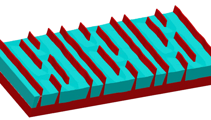
N7 FinFET Self-Aligned Quadruple Patterning Modeling
Read more
- N7 FinFET Self-Aligned Quadruple Patterning Modeling
N7 FinFET Self-Aligned Quadruple Patterning Modeling
(more…)
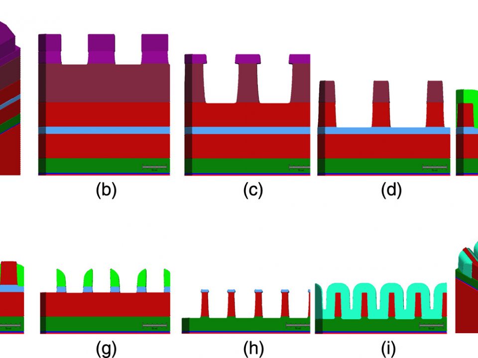
Self-Aligned Block and Fully Self-Aligned Via for iN5 Metal 2 Self-Aligned Quadruple Patterning
Read more
- Self-Aligned Block and Fully Self-Aligned Via for iN5 Metal 2 Self-Aligned Quadruple Patterning
Self-Aligned Block and Fully Self-Aligned Via for iN5 Metal 2 Self-Aligned Quadruple Patterning
(more…)
Modeling of Tone Inversion Process Flow for N5 Interconnect to Characterize Block Tip to Tip
Read more
- Modeling of Tone Inversion Process Flow for N5 Interconnect to Characterize Block Tip to Tip
Modeling of Tone Inversion Process Flow for N5 Interconnect to Characterize Block Tip to Tip
(more…)
Understanding how small variations in photoresist shape significantly impact multi-patterning yield
Read more
- Understanding how small variations in photoresist shape significantly impact multi-patterning yield
Understanding how small variations in photoresist shape significantly impact multi-patterning yield
(more…)
Optimizing DRAM Development using Directed Self-Assembly (DSA)
Read more
- Optimizing DRAM Development using Directed Self-Assembly (DSA)
Optimizing DRAM Development using Directed Self-Assembly (DSA)
(more…)
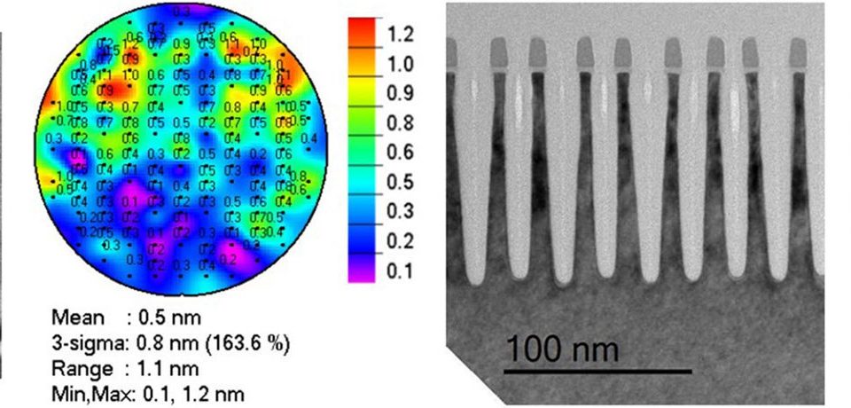
Self-aligned quadruple patterning to meet requirements for fins with high density
Read more
- Self-aligned quadruple patterning to meet requirements for fins with high density
Self-aligned quadruple patterning to meet requirements for fins with high density
(more…)
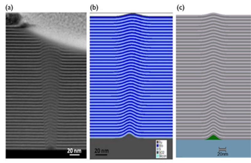
Defect Evolution in Next Generation, Extreme Ultraviolet Lithography
Read more
- Defect Evolution in Next Generation, Extreme Ultraviolet Lithography
Defect Evolution in Next Generation, Extreme Ultraviolet Lithography
(more…)
Back-End-of-Line (BEOL) Virtual Patterning
Read more
- Back-End-of-Line (BEOL) Virtual Patterning
Back-End-of-Line (BEOL) Virtual Patterning
(more…)
Contact Us
LOG IN
REGISTER