
Understanding how small variations in photoresist shape significantly impact multi-patterning yield
April 12, 2017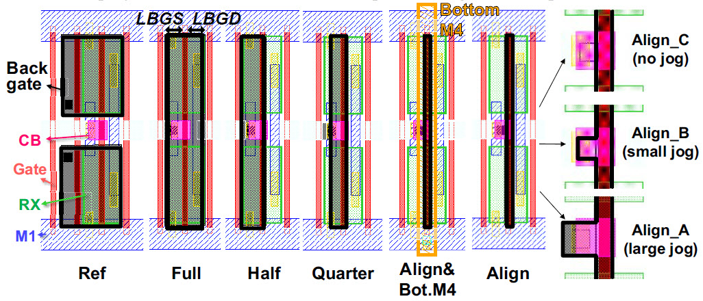
Design Technology Co-Optimization of 3D-monolithic standard cells and SRAM exploiting dynamic back-bias for ultra-low-voltage operation
December 29, 2017You must have an account on our Customer Portal to access this content. If you already have an account, please log in using the form below or to the right. If you do not have an account, we invite you to request an account.
Whitepaper: Modeling of Tone Inversion Process Flow for N5 Interconnect to Characterize Block Tip to Tip
To download your free white paper, please fill out the form below:
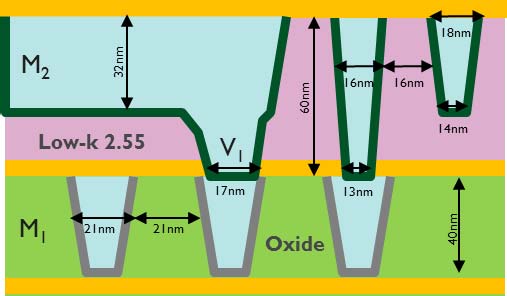
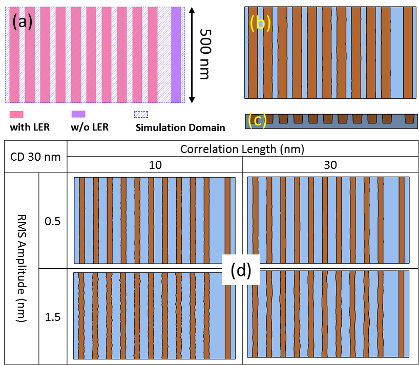
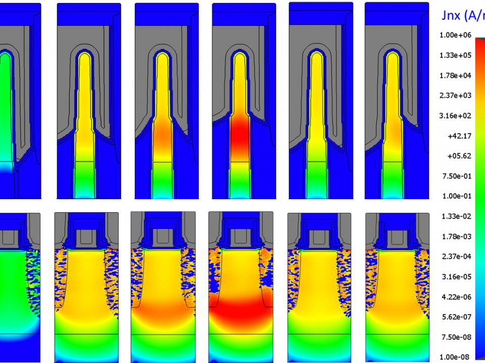
Abstract — Tip to Tip (T2T) of interconnect lines in advanced CMOS is quite important when downscaling the area of SRAM and logic standard cells. . When T2T size is increasing we have less space for via placement. Additionally variability could impact the yield of the Dual Damascene (DD) structure because of via placement or alignment. As we continue to extend 193i lithography for patterning block using multipatterning schemes, it is important to understand which processes have the most impact to T2T variability. In this paper we characterize the process window of key steps in a multi-patterning flow using Tone Inversion (TI) by studying the factors affecting CD in a T2T construct with 193i. We run a quantitative process window study of TI flow by using a DOE with emphasis on evolution of T2T dimension all completed on a virtual platform using COVENTOR SEMulator3D® tool. The virtual results were compared with 300mm silicon data processed at IMEC site with good agreement.
You might also be interested in:
- You must have an account on our Customer Portal to access this content. If you already have an account, please log in using the form below or to the right. […]
- You must have an account on our Customer Portal to access this content. If you already have an account, please log in using the form below or to the right. […]
- You must have an account on our Customer Portal to access this content. If you already have an account, please log in using the form below or to the right. […]
- You must have an account on our Customer Portal to access this content. If you already have an account, please log in using the form below or to the right. […]
- You must have an account on our Customer Portal to access this content. If you already have an account, please log in using the form below or to the right. […]
- You must have an account on our Customer Portal to access this content. If you already have an account, please log in using the form below or to the right. […]


