• Skip to main content
  • LOG IN
  • REGISTER
Lam_Research_logo_WhiteLam_Research_logo_WhiteLam_Research_logo_WhiteLam_Research_logo_White
  • Home
  • Customer Portal
    • Coventor Licensing Downloads
    • SEMulator3D Downloads
    • CoventorMP Downloads
    • Webinars
    • MEMS+ Courses
  • System Requirements
  • Software Licensing
Contact Us
✕
Figure 2: (a) Layout design, (b) Top view of a typical metal line generated, (c) cross sectional view of the metal line, (d) LER status of RMS and Correlation length split.
A Study of the Impact of Line Edge Roughness on Metal Line Resistance using Virtual Fabrication
August 18, 2022
Figure 2. Virtual metrology results for minimum and maximum area.

Figure 2. Virtual metrology results for minimum and maximum area.

You must have an account on our Customer Portal to access this content. If you already have an account, please log in using the form below or to the right. If you do not have an account, we invite you to request an account.

Existing Users Log In
   
Forgot password/username? Click here to reset
New User? Click here to register

Whitepaper: Pathfinding by process window modeling: Advanced DRAM capacitor patterning process window evaluation using virtual fabrication

fin-patterning-for-FinFETs

To download your free white paper, please fill out the form below:

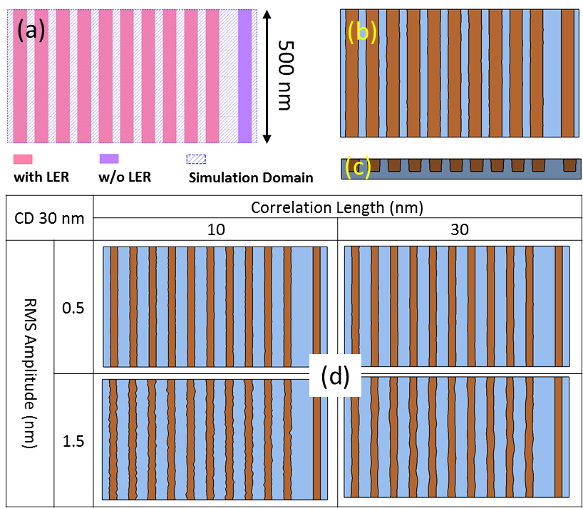
In advanced DRAM, capacitors with closely packed patterning are designed to increase cell density. Thus, advanced patterning schemes, such as multiple litho-etch, SADP and SAQP processes may be needed. In this paper, we systematically evaluate a DRAM capacitor hole formation process that includes SADP and SAQP patterning, using virtual fabrication and statistical analysis in SEMulator3D®. The purpose of this analysis is to obtain a quantified process window comparison between the SADP and SAQP patterning schemes.

© 2022 IEEE. Personal use of this material is permitted. Permission from IEEE must be obtained for all other uses, in any current or future media, including reprinting/republishing this material for advertising or promotional purposes, creating new collective works, for resale or redistribution to servers or lists, or reuse of any copyrighted component of this work in other works.

Share

You might also be interested in:

  • Pathfinding by process window modeling: Advanced DRAM capacitor patterning process window evaluation using virtual fabrication

    Read more - Pathfinding by process window modeling: Advanced DRAM capacitor patterning process window evaluation using virtual fabrication
    Figure 2. Virtual metrology results for minimum and maximum area.
    Pathfinding by process window modeling: Advanced DRAM capacitor patterning process window evaluation using virtual fabrication
    You must have an account on our Customer Portal to access this content. If you already have an account, please log in using the form below or to the right. […]
  • A Study of the Impact of Line Edge Roughness on Metal Line Resistance using Virtual Fabrication

    Read more - A Study of the Impact of Line Edge Roughness on Metal Line Resistance using Virtual Fabrication
    Figure 2: (a) Layout design, (b) Top view of a typical metal line generated, (c) cross sectional view of the metal line, (d) LER status of RMS and Correlation length split.
    A Study of the Impact of Line Edge Roughness on Metal Line Resistance using Virtual Fabrication
    You must have an account on our Customer Portal to access this content. If you already have an account, please log in using the form below or to the right. […]
  • Evaluating the Impact of STI Recess Profile Control on Advanced FinFET Device Performance

    Read more - Evaluating the Impact of STI Recess Profile Control on Advanced FinFET Device Performance
    Fig. 3: Leakage current distribution from different directions.
    Evaluating the Impact of STI Recess Profile Control on Advanced FinFET Device Performance
    You must have an account on our Customer Portal to access this content. If you already have an account, please log in using the form below or to the right. […]
  • The Effects of Poly Corner Etch Residue on Advanced FinFET Device Performance

    Read more - The Effects of Poly Corner Etch Residue on Advanced FinFET Device Performance
    Figure 3: On/off-state current distribution at fin bottom (top figures: no residue; bottom figure: with residue).
    The Effects of Poly Corner Etch Residue on Advanced FinFET Device Performance
    You must have an account on our Customer Portal to access this content. If you already have an account, please log in using the form below or to the right. […]
  • SVT (six stacked vertical transistors) SRAM cell architecture introduction: design and process challenges assessment

    Read more - SVT (six stacked vertical transistors) SRAM cell architecture introduction: design and process challenges assessment
    Figure 4: Four different process/design changes introduced for the second investigation path of SSVT-SRAM virtual fabrication.
    SVT (six stacked vertical transistors) SRAM cell architecture introduction: design and process challenges assessment
    You must have an account on our Customer Portal to access this content. If you already have an account, please log in using the form below or to the right. […]
  • A Triple-Deck CFET Structure with an Integrated SRAM Cell for the 2nm Technology Node and Beyond

    Read more - A Triple-Deck CFET Structure with an Integrated SRAM Cell for the 2nm Technology Node and Beyond
    fig-6-process-flow-for-separation-gate-of-pass-gate-transistor
    A Triple-Deck CFET Structure with an Integrated SRAM Cell for the 2nm Technology Node and Beyond
    You must have an account on our Customer Portal to access this content. If you already have an account, please log in using the form below or to the right. […]
Share

Related posts

Figure 2: (a) Layout design, (b) Top view of a typical metal line generated, (c) cross sectional view of the metal line, (d) LER status of RMS and Correlation length split.

Figure 2: (a) Layout design, (b) Top view of a typical metal line generated, (c) cross sectional view of the metal line, (d) LER status of RMS and Correlation length split.

August 18, 2022

A Study of the Impact of Line Edge Roughness on Metal Line Resistance using Virtual Fabrication


Read more - A Study of the Impact of Line Edge Roughness on Metal Line Resistance using Virtual Fabrication
Fig. 3: Leakage current distribution from different directions.

Fig. 3: Leakage current distribution from different directions.

September 14, 2021

Evaluating the Impact of STI Recess Profile Control on Advanced FinFET Device Performance


Read more - Evaluating the Impact of STI Recess Profile Control on Advanced FinFET Device Performance
Figure 3: On/off-state current distribution at fin bottom (top figures: no residue; bottom figure: with residue).

Figure 3: On/off-state current distribution at fin bottom (top figures: no residue; bottom figure: with residue).

June 16, 2021

The Effects of Poly Corner Etch Residue on Advanced FinFET Device Performance


Read more - The Effects of Poly Corner Etch Residue on Advanced FinFET Device Performance
Figure 4: Four different process/design changes introduced for the second investigation path of SSVT-SRAM virtual fabrication.

Figure 4: Four different process/design changes introduced for the second investigation path of SSVT-SRAM virtual fabrication.

March 8, 2021

SVT (six stacked vertical transistors) SRAM cell architecture introduction: design and process challenges assessment


Read more - SVT (six stacked vertical transistors) SRAM cell architecture introduction: design and process challenges assessment
© LAM RESEARCH CORPORATION. ALL RIGHTS RESERVED.
    Contact Us
    • LOG IN
    • REGISTER