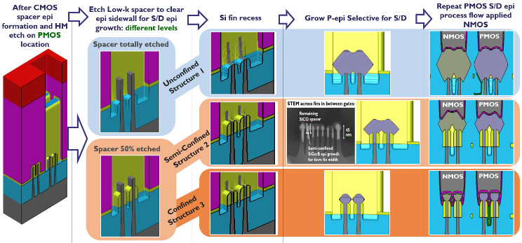
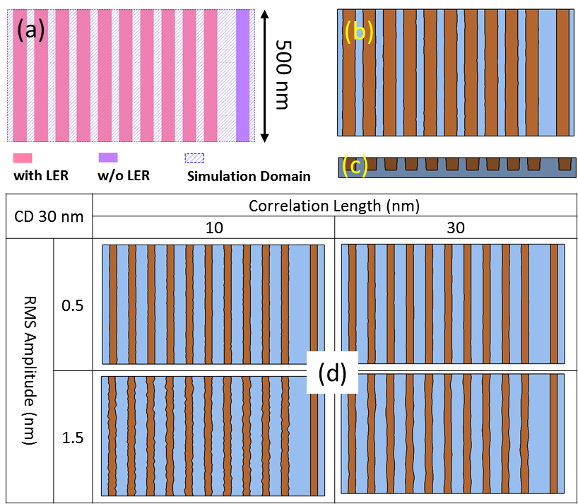
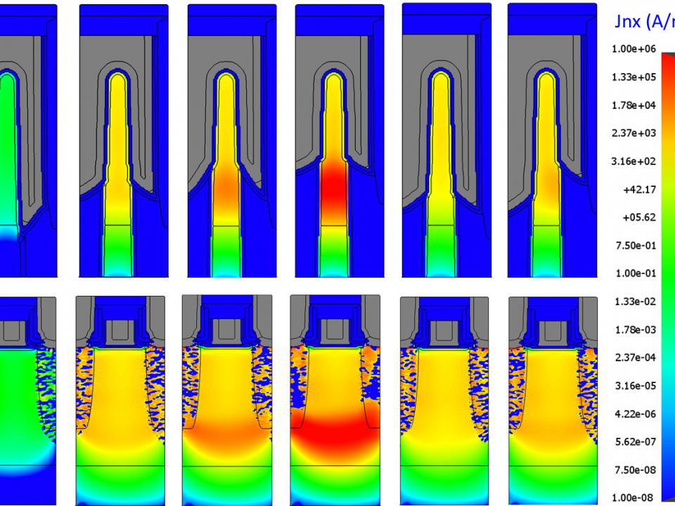
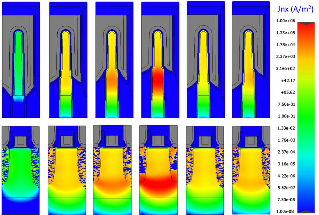
Evaluation of the impact of source drain epi implementation on logic performance using combined process and circuit simulation
December 16, 2020
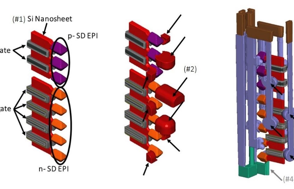
SVT (six stacked vertical transistors) SRAM cell architecture introduction: design and process challenges assessment
March 8, 2021You must have an account on our Customer Portal to access this content. If you already have an account, please log in using the form below or to the right. If you do not have an account, we invite you to request an account.
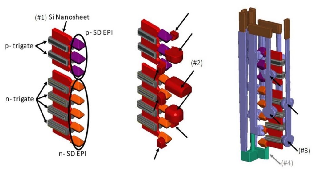
Whitepaper: A Triple-Deck CFET Structure with an Integrated SRAM Cell for the 2nm Technology Node and Beyond

To download your free white paper, please fill out the form below:
A novel triple-deck CFET structure is proposed for the first time as a candidate for area scaling. The proposed triple-deck CFET aggressively stacks a pass gate over an inverter to form a half SRAM bit cell. The integration flow and full metal connectivity have been carefully designed for functionality and array assembly. Most of the pitch used in the process is around 40nm, which is patternable using 193i litho process to reduce patterning cost and difficulty. We have also studied parasitic capacitance and resistance to evaluate design weakness of the proposed structure.
You might also be interested in:
- You must have an account on our Customer Portal to access this content. If you already have an account, please log in using the form below or to the right. […]
- You must have an account on our Customer Portal to access this content. If you already have an account, please log in using the form below or to the right. […]
- You must have an account on our Customer Portal to access this content. If you already have an account, please log in using the form below or to the right. […]
- You must have an account on our Customer Portal to access this content. If you already have an account, please log in using the form below or to the right. […]
- You must have an account on our Customer Portal to access this content. If you already have an account, please log in using the form below or to the right. […]
- You must have an account on our Customer Portal to access this content. If you already have an account, please log in using the form below or to the right. […]

