Skip to main content
LOG IN
REGISTER
Home
Customer Portal
Coventor Licensing Downloads
SEMulator3D Downloads
CoventorMP Downloads
Webinars
MEMS+ Courses
System Requirements
Software Licensing
Contact Us
✕
Enter your search
(more…)
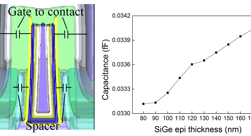
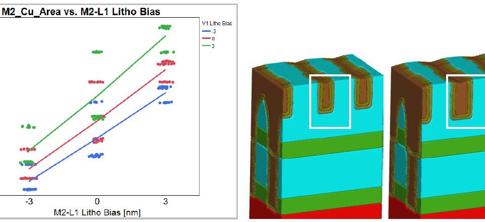
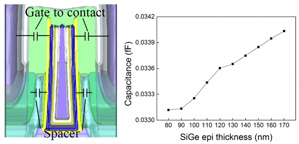
Influence of SiGe on Parasitic Parameters in PMOS
Read more
- Influence of SiGe on Parasitic Parameters in PMOS
Influence of SiGe on Parasitic Parameters in PMOS
(more…)
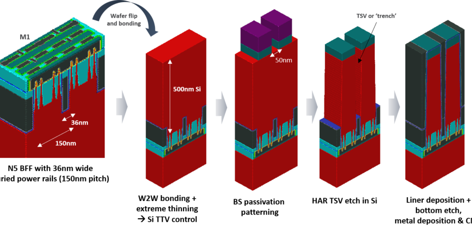
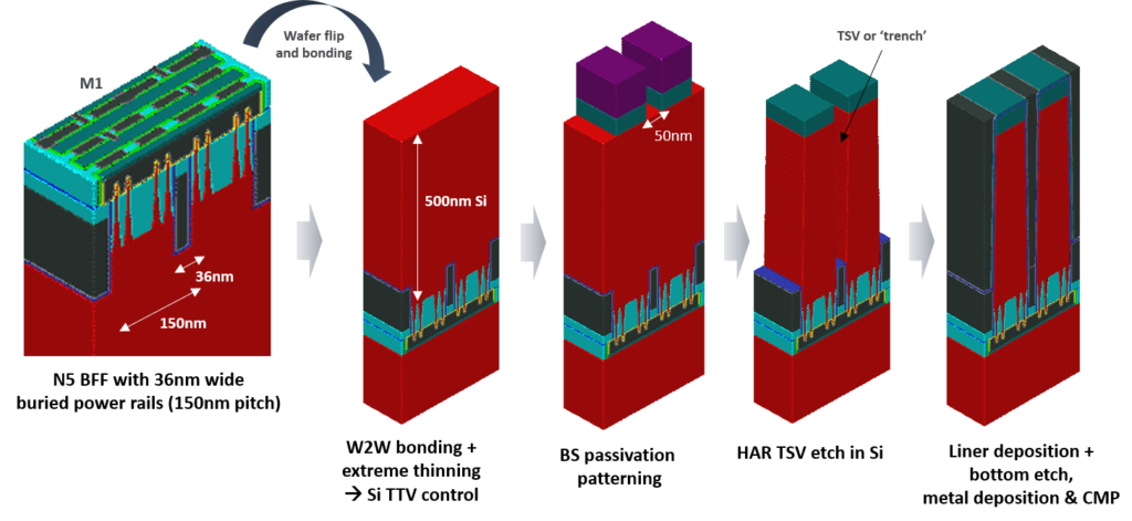
Backside Power Delivery as a Scaling Knob for Future Systems
Read more
- Backside Power Delivery as a Scaling Knob for Future Systems
Backside Power Delivery as a Scaling Knob for Future Systems
(more…)
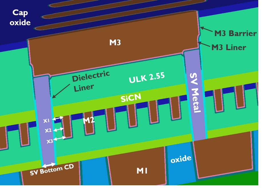
CMOS Area Scaling and the Need for High Aspect Ratio Vias
Read more
- CMOS Area Scaling and the Need for High Aspect Ratio Vias
CMOS Area Scaling and the Need for High Aspect Ratio Vias
(more…)
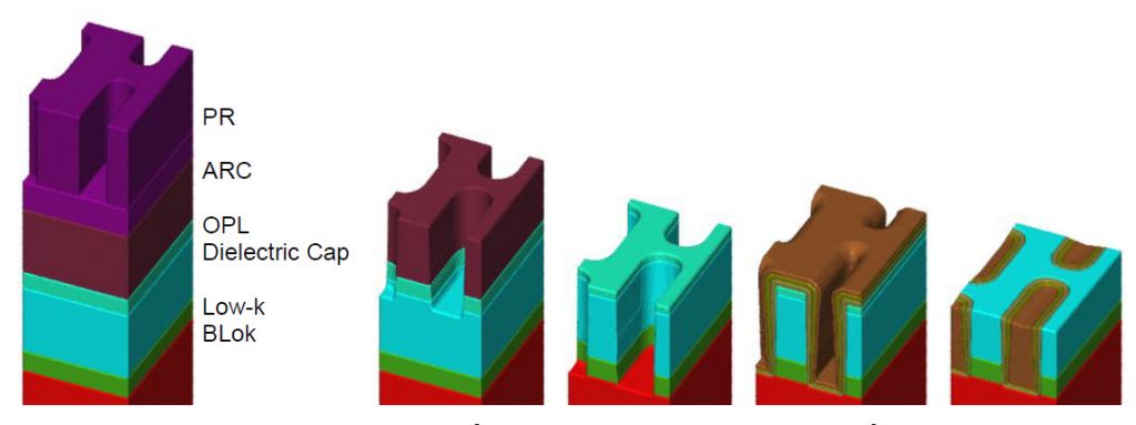
Back-End-of-Line (BEOL) Metallization
Read more
- Back-End-of-Line (BEOL) Metallization
Back-End-of-Line (BEOL) Metallization
(more…)
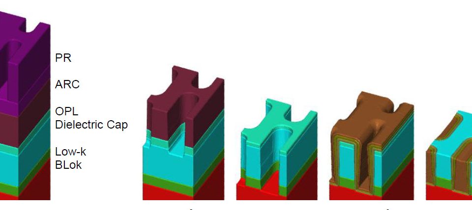
Back-End-of-Line (BEOL) Virtual Patterning
Read more
- Back-End-of-Line (BEOL) Virtual Patterning
Back-End-of-Line (BEOL) Virtual Patterning
(more…)
Contact Us
LOG IN
REGISTER