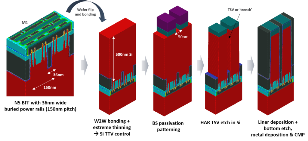
Backside Power Delivery as a Scaling Knob for Future Systems
July 3, 2019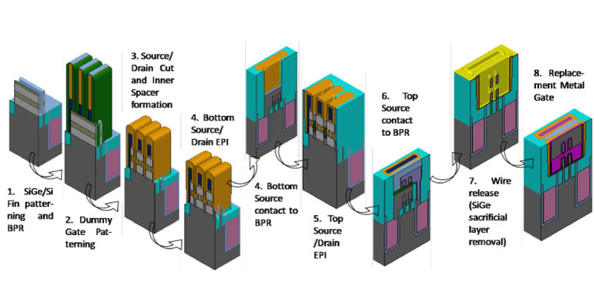
A Benchmark Study of Complementary-Field Effect Transistor (CFET) Process Integration Options: Comparing Bulk vs. SOI vs. DSOI Starting Substrates
November 15, 2019You must have an account on our Customer Portal to access this content. If you already have an account, please log in using the form below or to the right. If you do not have an account, we invite you to request an account.
Whitepaper: Influence of SiGe on Parasitic Parameters in PMOS

To download your free white paper, please fill out the form below:
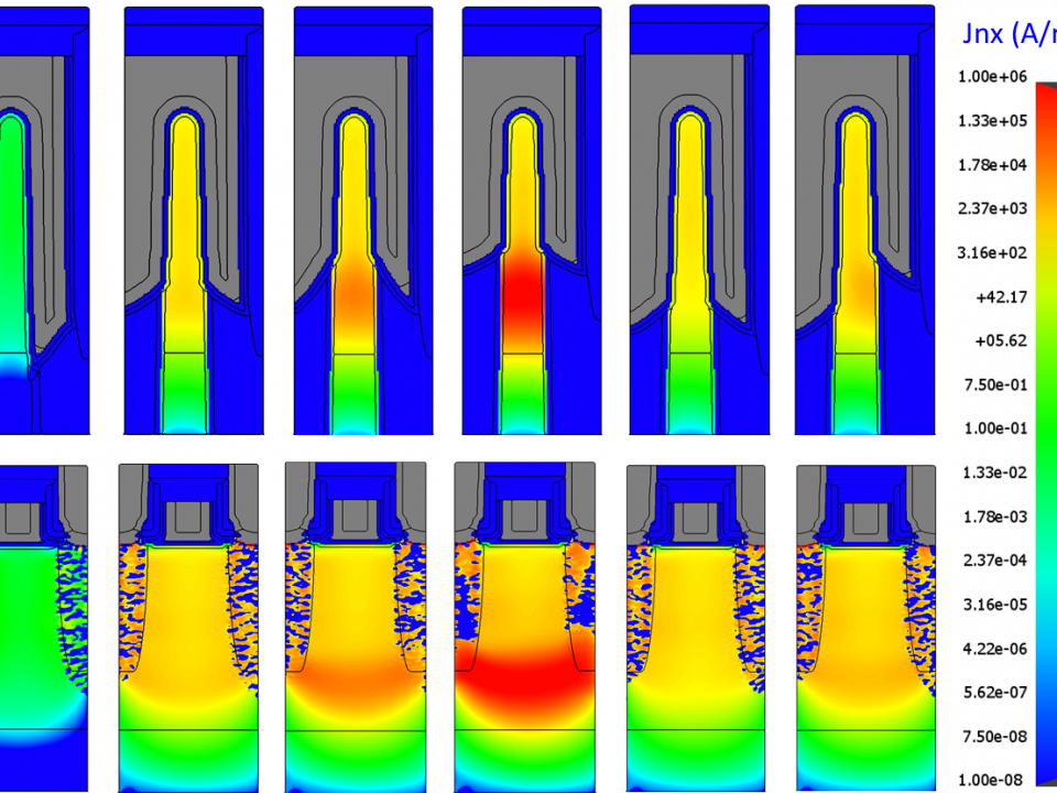
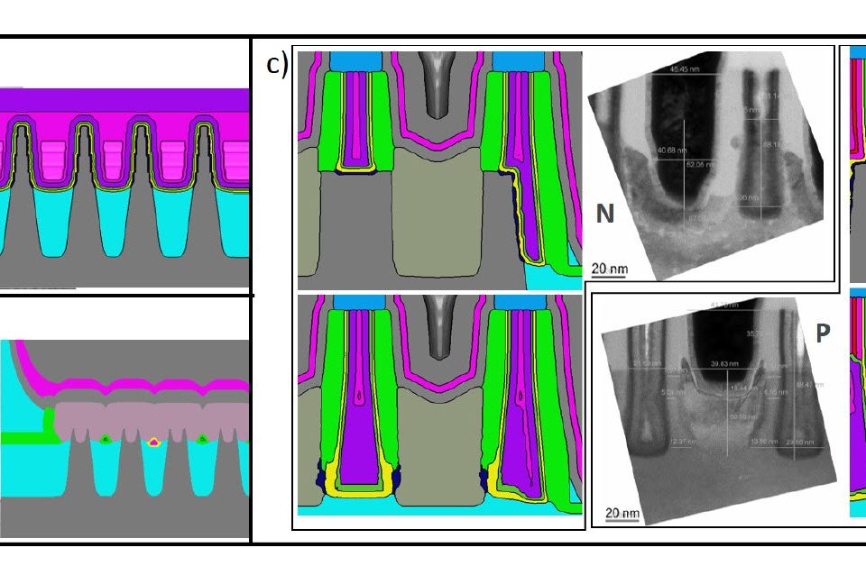
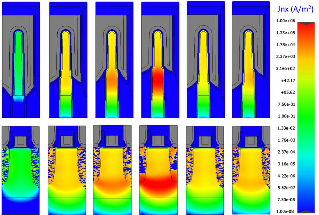
In this paper, simulation-based design-technology co-optimization (DTCO) is carried out using the Coventor SEMulator3D virtual fabrication platform with its integrated electrical analysis capabilities [1]. In our study, process modeling is used to predict the sensitivity of FinFET device performance to changes in a silicon germanium epitaxial process. The simulated process is a gate-last flow process applied to a 14nm FinFET. The source drain contact resistance and fringing capacitance are extracted to examine the effect of process changes on device performance. Finally, TCAD simulation is adopted to complete the transistor level simulation.
You might also be interested in:
- You must have an account on our Customer Portal to access this content. If you already have an account, please log in using the form below or to the right. […]
- You must have an account on our Customer Portal to access this content. If you already have an account, please log in using the form below or to the right. […]
- You must have an account on our Customer Portal to access this content. If you already have an account, please log in using the form below or to the right. […]
- You must have an account on our Customer Portal to access this content. If you already have an account, please log in using the form below or to the right. […]
- You must have an account on our Customer Portal to access this content. If you already have an account, please log in using the form below or to the right. […]
- You must have an account on our Customer Portal to access this content. If you already have an account, please log in using the form below or to the right. […]


