Process Modeling Exploration for 8 nm Half-Pitch Interconnects
February 1, 2019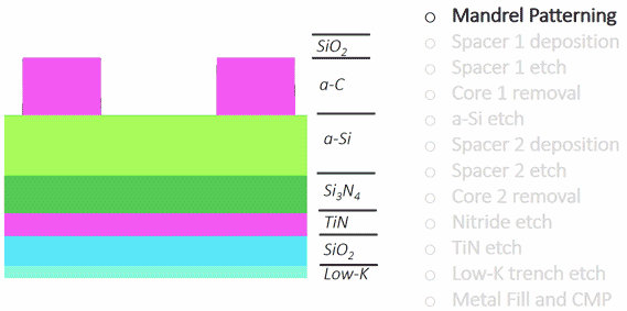
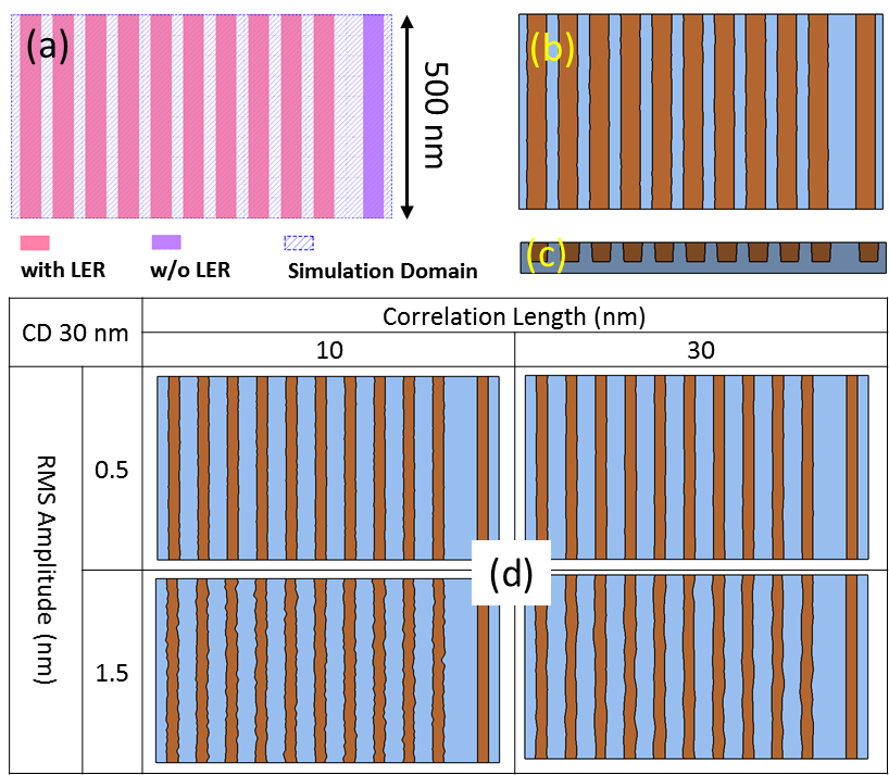
Virtual Fabrication and Advanced Process Control Improve Yield for SAQP Process Assessment with 16 nm Half-Pitch
March 21, 2019You must have an account on our Customer Portal to access this content. If you already have an account, please log in using the form below or to the right. If you do not have an account, we invite you to request an account.
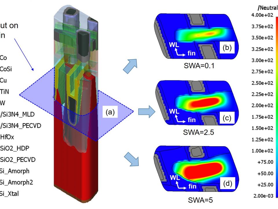
Whitepaper: CMOS Area Scaling and the Need for High Aspect Ratio Vias

To download your free white paper, please fill out the form below:
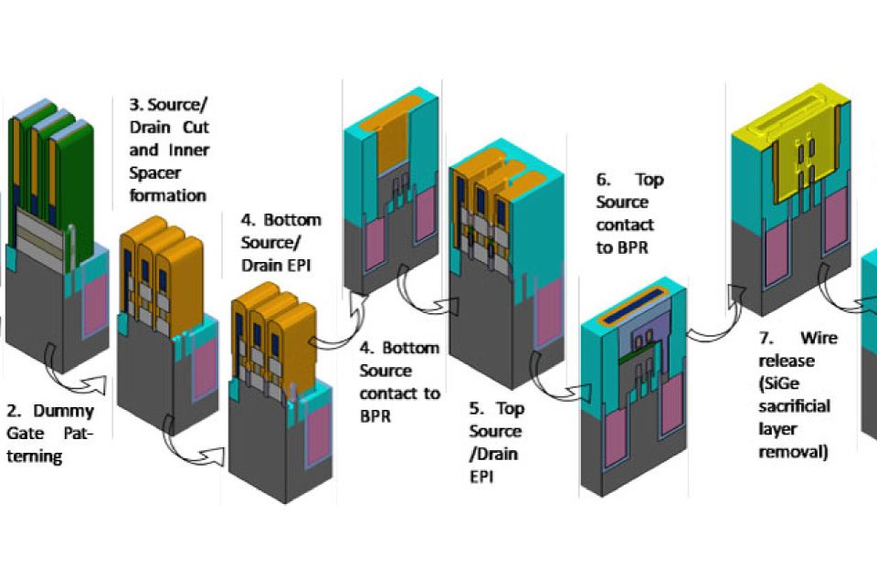
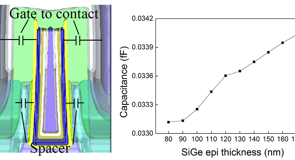
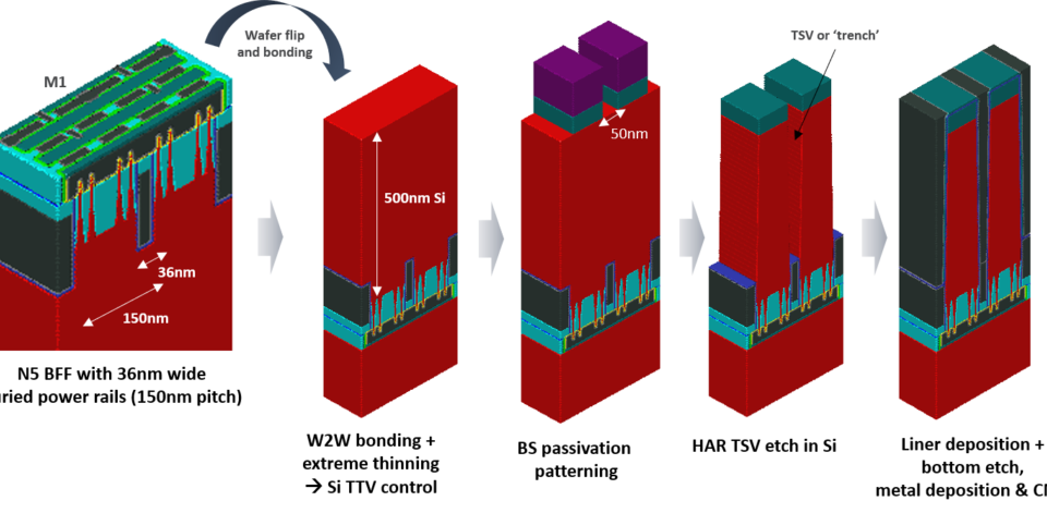
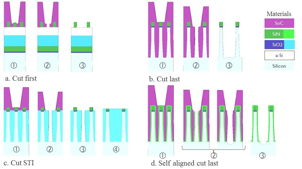
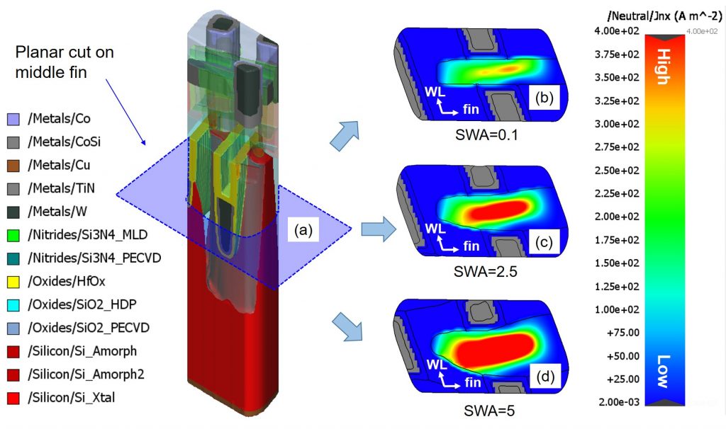
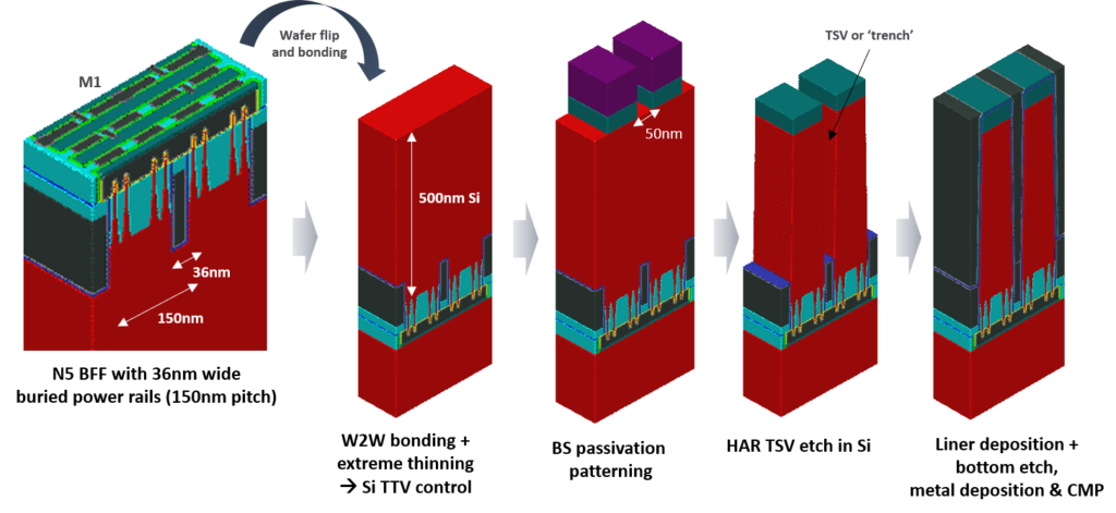
Resolving internal routing congestion will be essential to enable CMOS area scaling to the N5 node and beyond. The solution will require new design maneuvers in place and route (PnR), as well as patterning innovations. In this work, we present inter-layer high aspect ratio vias or ‘SuperVia’ (SV) as one technology element that could enable track height scaling to 4.5T at aggressive N5 dimensions. We present morphological results of the patterning scheme and discuss the impact of process variations on SV resistance obtained from empirical resistance simulations.
You might also be interested in:
- You must have an account on our Customer Portal to access this content. If you already have an account, please log in using the form below or to the right. […]
- You must have an account on our Customer Portal to access this content. If you already have an account, please log in using the form below or to the right. […]
- You must have an account on our Customer Portal to access this content. If you already have an account, please log in using the form below or to the right. […]
- You must have an account on our Customer Portal to access this content. If you already have an account, please log in using the form below or to the right. […]
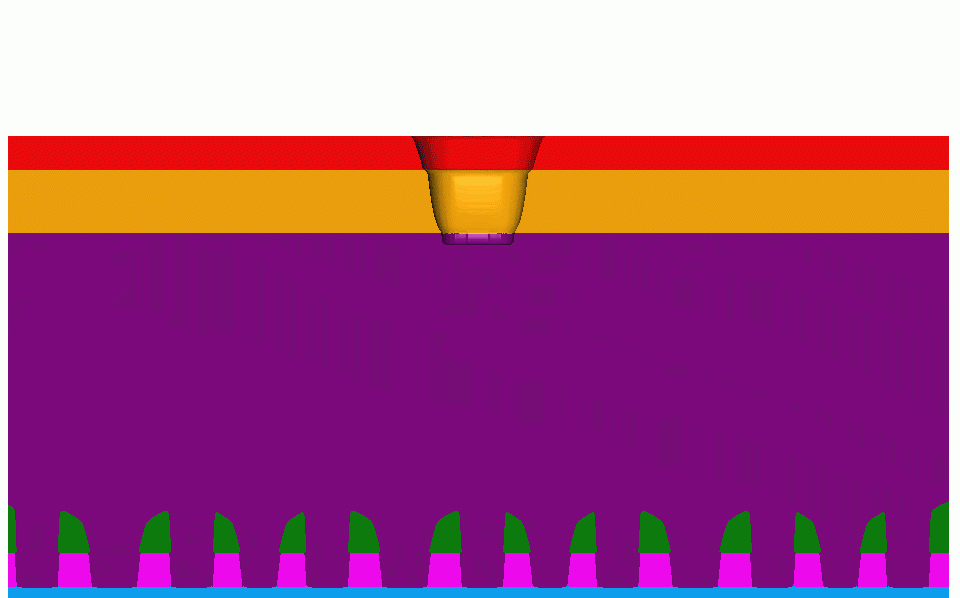
Impact of EUV Resist Thickness on Local Critical Dimension Uniformities for <30 nm CD Via Patterning
Impact of EUV Resist Thickness on Local Critical Dimension Uniformities for <30 nm CD Via Patterning
You must have an account on our Customer Portal to access this content. If you already have an account, please log in using the form below or to the right. […]- You must have an account on our Customer Portal to access this content. If you already have an account, please log in using the form below or to the right. […]
- You must have an account on our Customer Portal to access this content. If you already have an account, please log in using the form below or to the right. […]
- You must have an account on our Customer Portal to access this content. If you already have an account, please log in using the form below or to the right. […]
- You must have an account on our Customer Portal to access this content. If you already have an account, please log in using the form below or to the right. […]
- You must have an account on our Customer Portal to access this content. If you already have an account, please log in using the form below or to the right. […]
- You must have an account on our Customer Portal to access this content. If you already have an account, please log in using the form below or to the right. […]
- You must have an account on our Customer Portal to access this content. If you already have an account, please log in using the form below or to the right. […]

