Skip to main content
LOG IN
REGISTER
Home
Customer Portal
Coventor Licensing Downloads
SEMulator3D Downloads
CoventorMP Downloads
Webinars
MEMS+ Courses
System Requirements
Software Licensing
Contact Us
✕
Enter your search
(more…)
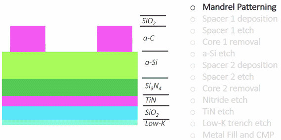
Virtual Fabrication and Advanced Process Control Improve Yield for SAQP Process Assessment with 16 nm Half-Pitch
Read more
- Virtual Fabrication and Advanced Process Control Improve Yield for SAQP Process Assessment with 16 nm Half-Pitch
Virtual Fabrication and Advanced Process Control Improve Yield for SAQP Process Assessment with 16 nm Half-Pitch
(more…)
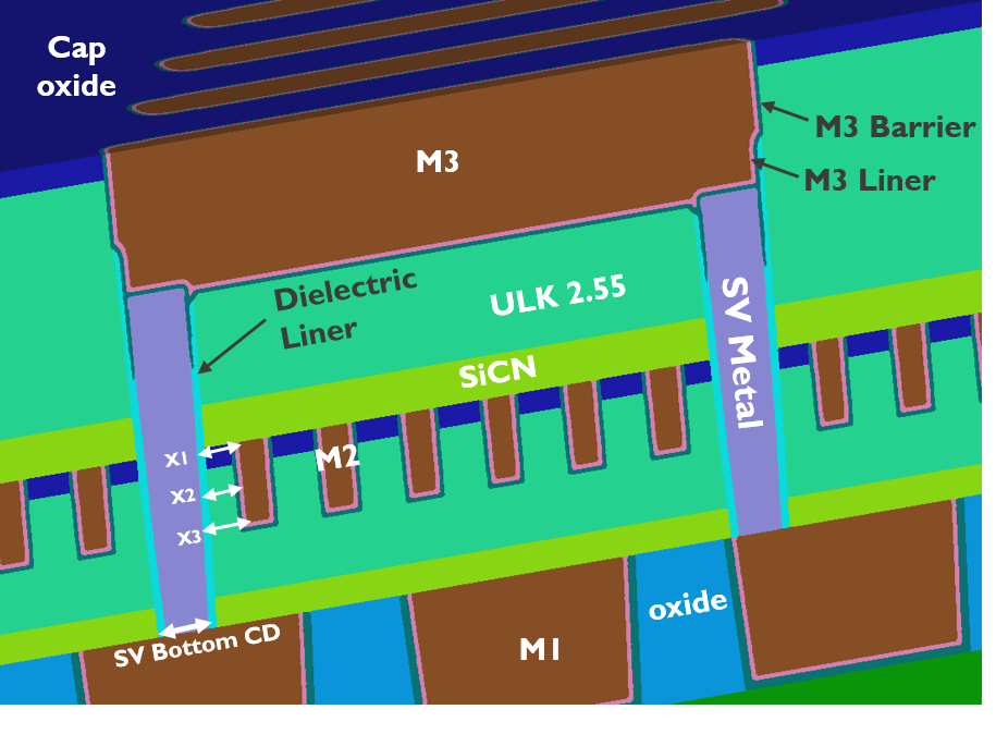
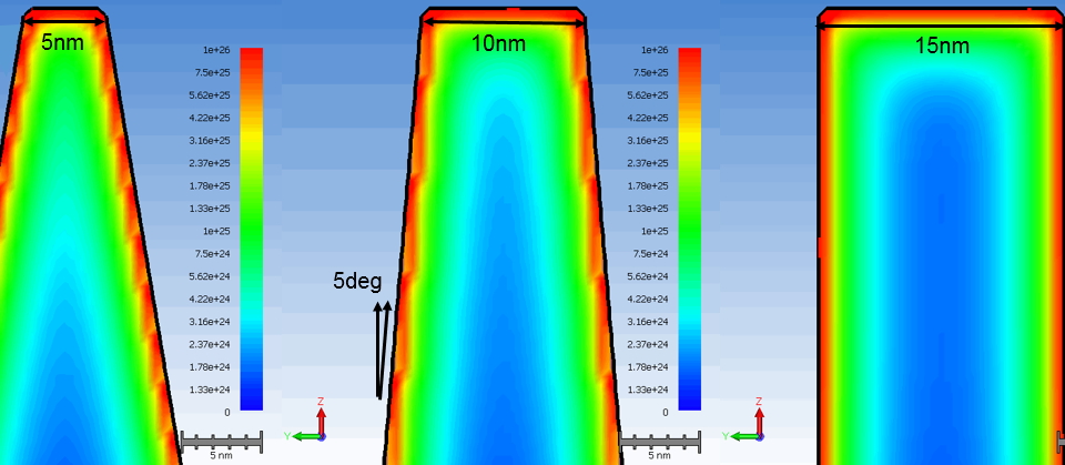
CMOS Area Scaling and the Need for High Aspect Ratio Vias
Read more
- CMOS Area Scaling and the Need for High Aspect Ratio Vias
CMOS Area Scaling and the Need for High Aspect Ratio Vias
(more…)
Process Modeling Exploration for 8 nm Half-Pitch Interconnects
Read more
- Process Modeling Exploration for 8 nm Half-Pitch Interconnects
Process Modeling Exploration for 8 nm Half-Pitch Interconnects
(more…)
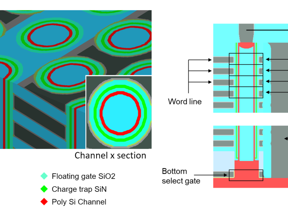
Innovative Solutions to Increase 3D NAND Flash Memory Density
Read more
- Innovative Solutions to Increase 3D NAND Flash Memory Density
Innovative Solutions to Increase 3D NAND Flash Memory Density
(more…)
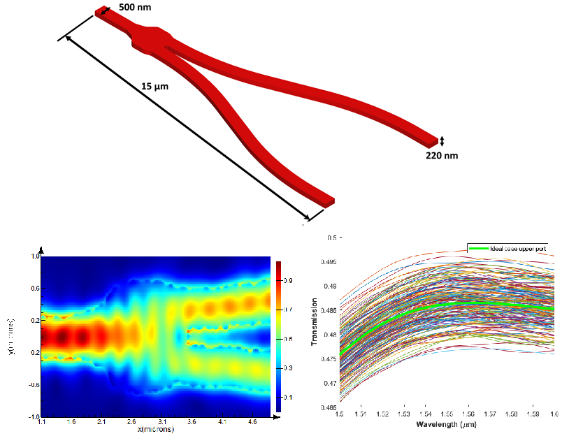
Effects of a Random Process Variation on the Transfer Characteristics of a Fundamental Photonic Integrated Circuit Component
Read more
- Effects of a Random Process Variation on the Transfer Characteristics of a Fundamental Photonic Integrated Circuit Component
Effects of a Random Process Variation on the Transfer Characteristics of a Fundamental Photonic Integrated Circuit Component
(more…)
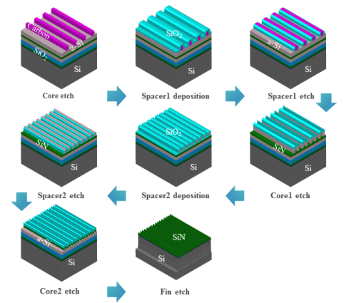
N7 FinFET Self-Aligned Quadruple Patterning Modeling
Read more
- N7 FinFET Self-Aligned Quadruple Patterning Modeling
N7 FinFET Self-Aligned Quadruple Patterning Modeling
(more…)
Understanding the Effect of Variability in Bulk FinFET Device Performance
Read more
- Understanding the Effect of Variability in Bulk FinFET Device Performance
Understanding the Effect of Variability in Bulk FinFET Device Performance
(more…)
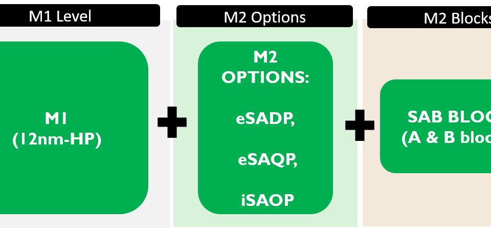
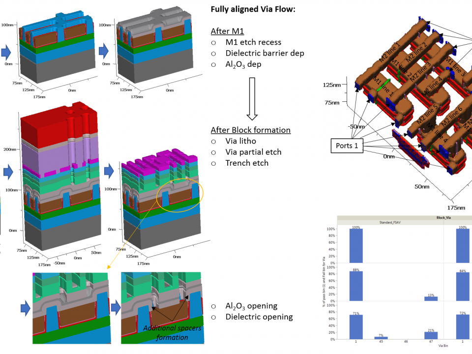
Self-Aligned Block and Fully Self-Aligned Via for iN5 Metal 2 Self-Aligned Quadruple Patterning
Read more
- Self-Aligned Block and Fully Self-Aligned Via for iN5 Metal 2 Self-Aligned Quadruple Patterning
Self-Aligned Block and Fully Self-Aligned Via for iN5 Metal 2 Self-Aligned Quadruple Patterning
(more…)
Design Technology Co-Optimization of 3D-monolithic standard cells and SRAM exploiting dynamic back-bias for ultra-low-voltage operation
Read more
- Design Technology Co-Optimization of 3D-monolithic standard cells and SRAM exploiting dynamic back-bias for ultra-low-voltage operation
Design Technology Co-Optimization of 3D-monolithic standard cells and SRAM exploiting dynamic back-bias for ultra-low-voltage operation
(more…)
Load more
Contact Us
LOG IN
REGISTER