Process Variation Analysis of Device Performance Using Virtual Fabrication: Methodology Demonstrated on a CMOS 14-nm FinFET Vehicle
November 30, 2020
A Triple-Deck CFET Structure with an Integrated SRAM Cell for the 2nm Technology Node and Beyond
January 19, 2021You must have an account on our Customer Portal to access this content. If you already have an account, please log in using the form below or to the right. If you do not have an account, we invite you to request an account.
Whitepaper: Evaluation of the impact of source drain epi implementation on logic performance using combined process and circuit simulation
To download your free white paper, please fill out the form below:
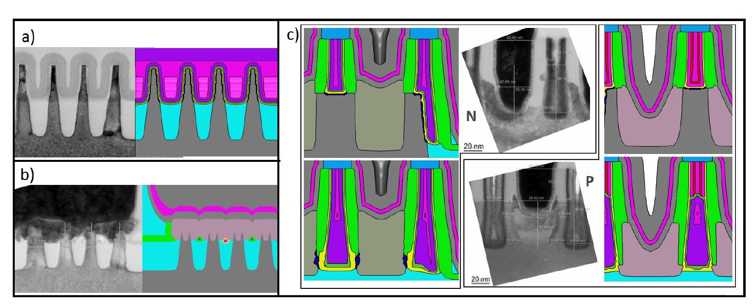
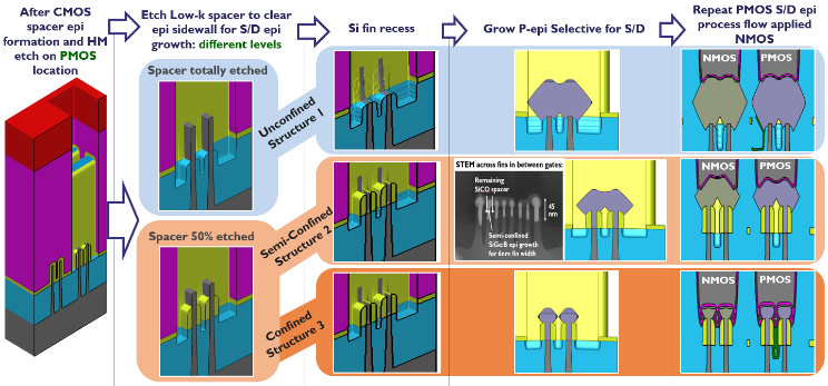
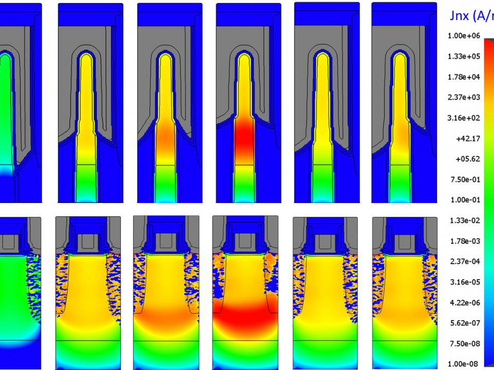
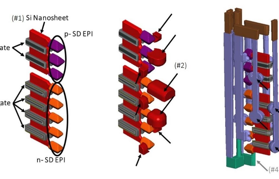
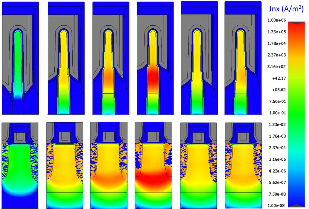
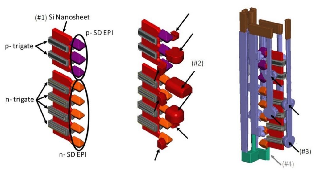
In this paper, we explore an end-to-end solution using SEMulator3D® [1] to address the need to include process variation effects in circuit simulation. For the first time, we couple SEMulator3D with BSIM compact modeling to evaluate process variation impacts on circuit performance. The process integration goal of the study was to optimize contacts and spacer thickness of advanced-node FinFETs in term of speed and power performance. To do so, we compare three structures with different spacer recess levels and epi shape growth profiles. We investigate the effect of low-k spacer thickness variation to select the best combination of spacer thickness and S/D epi shape to improve speed and power performance.
You might also be interested in:
- You must have an account on our Customer Portal to access this content. If you already have an account, please log in using the form below or to the right. […]
- You must have an account on our Customer Portal to access this content. If you already have an account, please log in using the form below or to the right. […]
- You must have an account on our Customer Portal to access this content. If you already have an account, please log in using the form below or to the right. […]
- You must have an account on our Customer Portal to access this content. If you already have an account, please log in using the form below or to the right. […]
- You must have an account on our Customer Portal to access this content. If you already have an account, please log in using the form below or to the right. […]
- You must have an account on our Customer Portal to access this content. If you already have an account, please log in using the form below or to the right. […]

