
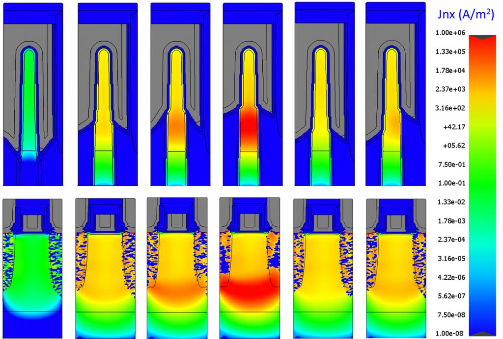
Impact of EUV Resist Thickness on Local Critical Dimension Uniformities for <30 nm CD Via Patterning
March 30, 2020
Process Model Calibration: The Key to Building Predictive and Accurate 3D Process Models
July 21, 2020You must have an account on our Customer Portal to access this content. If you already have an account, please log in using the form below or to the right. If you do not have an account, we invite you to request an account.
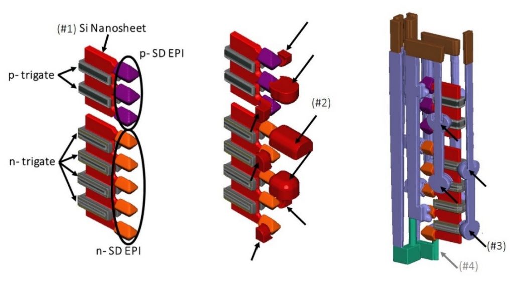
Whitepaper: A Benchmark Study of Complementary-Field Effect Transistor (CFET) Process Integration Options done by Virtual Fabrication
To download your free white paper, please fill out the form below:
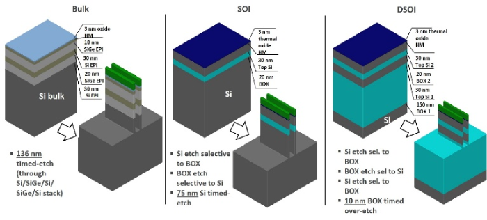
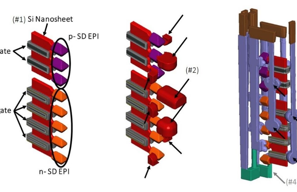
Four process flow options for Complementary-Field Effect Transistors (C-FET), using different designs and starting substrates (Si bulk, Silicon-On-Insulator, or Double-SOI), were compared to assess the probability of process variation failures. The study was performed using virtual fabrication techniques without requiring fabrication of any actual test wafers. In the study, Nanosheet-on-Nanosheet stacked channels provided superior process integration robustness compared to Nanowire-On-Fin stacked channels. For the Nanowire-On-Fin option, using an SOI substrate as the starting material (compared to Si bulk or DSOI) also strongly reduced process variation failure rates.
© 2020 IEEE. Personal use of this material is permitted. Permission from IEEE must be obtained for all other uses, in any current or future media, including reprinting/republishing this material for advertising or promotional purposes, creating new collective works, for resale or redistribution to servers or lists, or reuse of any copyrighted component of this work in other works. Published in: IEEE Journal of the Electron Devices Society ( Early Access ).
DOI: 10.1109/JEDS.2020.2990718
You might also be interested in:
- You must have an account on our Customer Portal to access this content. If you already have an account, please log in using the form below or to the right. […]
- You must have an account on our Customer Portal to access this content. If you already have an account, please log in using the form below or to the right. […]
- You must have an account on our Customer Portal to access this content. If you already have an account, please log in using the form below or to the right. […]
- You must have an account on our Customer Portal to access this content. If you already have an account, please log in using the form below or to the right. […]
- You must have an account on our Customer Portal to access this content. If you already have an account, please log in using the form below or to the right. […]
- You must have an account on our Customer Portal to access this content. If you already have an account, please log in using the form below or to the right. […]


