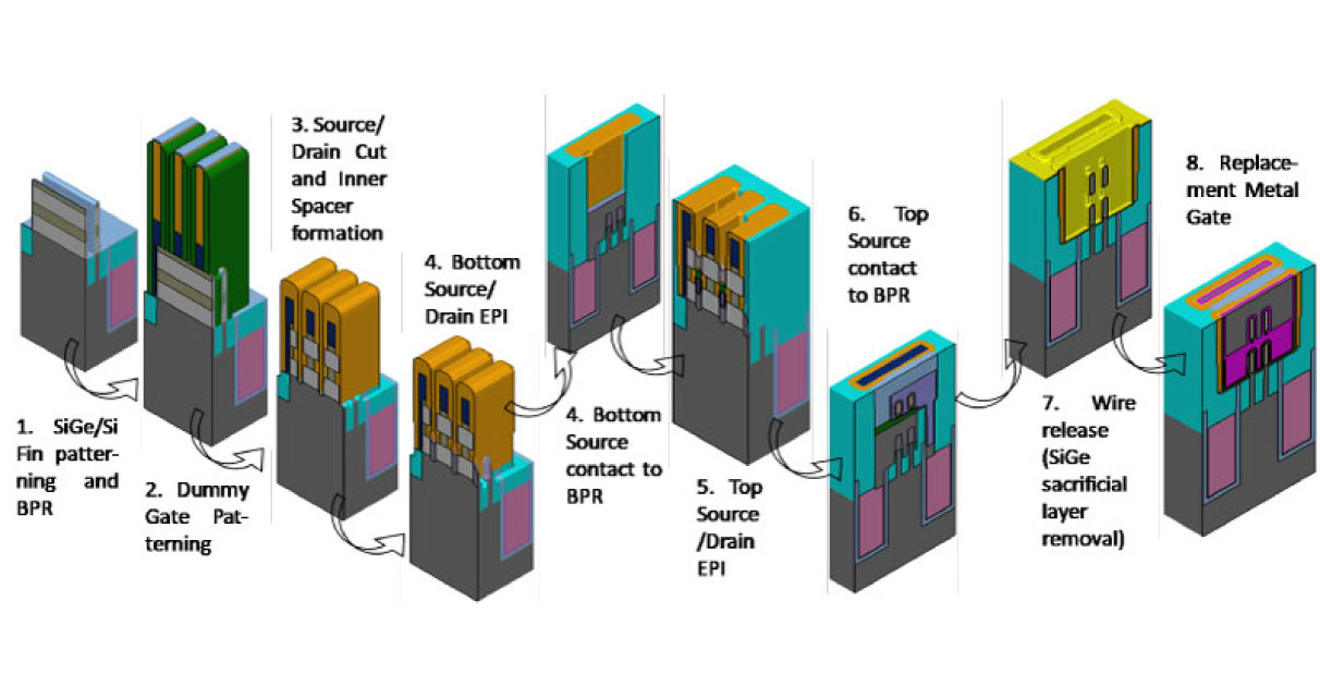
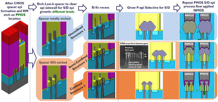
A Benchmark Study of Complementary-Field Effect Transistor (CFET) Process Integration Options: Comparing Bulk vs. SOI vs. DSOI Starting Substrates
November 15, 2019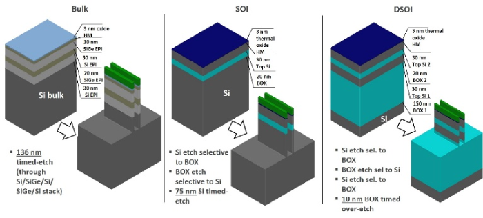
A Benchmark Study of Complementary-Field Effect Transistor (CFET) Process Integration Options done by Virtual Fabrication
May 26, 2020You must have an account on our Customer Portal to access this content. If you already have an account, please log in using the form below or to the right. If you do not have an account, we invite you to request an account.
Whitepaper: Impact of EUV Resist Thickness on Local Critical Dimension Uniformities for <30 nm CD Via Patterning

To download your free white paper, please fill out the form below:
This paper describes the impact of Extreme Ultraviolet (EUV) resist thickness on <30 nm Via Local Critical Dimension Uniformity (LCDU) measured during After Development Inspection (ADI) and After Etch Inspection (AEI). For the same post-etch CD targets, increasing resist thickness from 40 to 60 nm helped reduced CD variability. This work was performed via virtual fabrication using Coventor’s SEMulator3D® software and was confirmed experimentally. Post litho and post etch CD variations were introduced by considering lithography dose and focus variations in the model. Lithography and etch models were calibrated using 3D resist profile simulations from HyperLith® and post-etch Cross Section Scanning Electron Microscope (XSEM) images, respectively.
© 2020 IEEE. Personal use of this material is permitted. Permission from IEEE must be obtained for all other uses, in any current or future media, including reprinting/republishing this material for advertising or promotional purposes, creating new collective works, for resale or redistribution to servers or lists, or reuse of any copyrighted component of this work in other works.
B. Vincent, M. J. Maslow, J. Bekaert, M. Mao, and J. Ervin "Impact of EUV resist thickness on local critical dimension uniformities for 30
You might also be interested in:
- You must have an account on our Customer Portal to access this content. If you already have an account, please log in using the form below or to the right. […]
- You must have an account on our Customer Portal to access this content. If you already have an account, please log in using the form below or to the right. […]
- You must have an account on our Customer Portal to access this content. If you already have an account, please log in using the form below or to the right. […]
- You must have an account on our Customer Portal to access this content. If you already have an account, please log in using the form below or to the right. […]
- You must have an account on our Customer Portal to access this content. If you already have an account, please log in using the form below or to the right. […]
- You must have an account on our Customer Portal to access this content. If you already have an account, please log in using the form below or to the right. […]


