A Study of Wiggling AA Modeling and its Impact on Device Performance in Advanced DRAM
October 23, 2020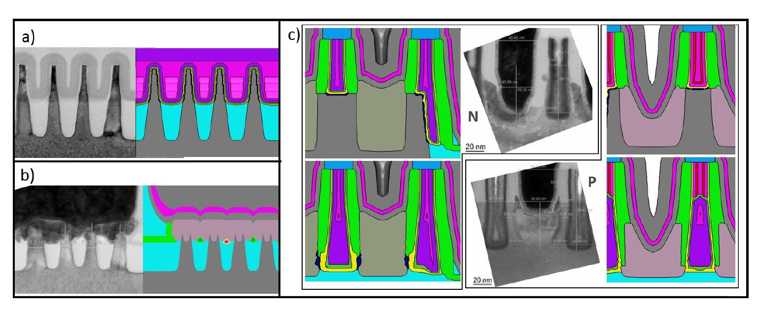
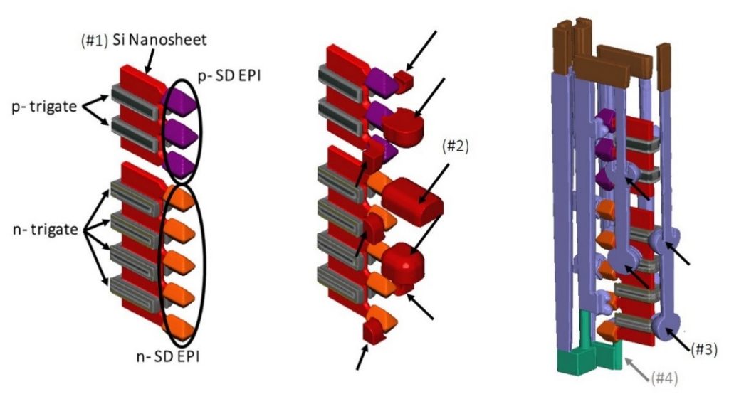
Process Variation Analysis of Device Performance Using Virtual Fabrication: Methodology Demonstrated on a CMOS 14-nm FinFET Vehicle
November 30, 2020You must have an account on our Customer Portal to access this content. If you already have an account, please log in using the form below or to the right. If you do not have an account, we invite you to request an account.
Whitepaper: Process Window Optimization of DRAM by Virtual Fabrication
To download your free white paper, please fill out the form below:
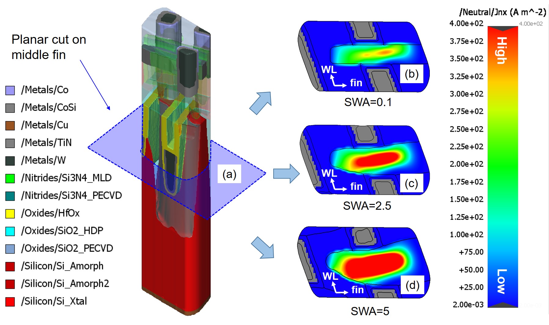
As advanced CMOS scaling and new memory technology development moves forward, increasingly complex and vertical structures cause unexpected challenges in manufacturing and yield. In 3D NAND flash memory, to reduce bit costs and increase chip densities, stacks higher than 192 layers with multi-tier schemes are under development. This, however, casts unprecedented challenges for etching high aspect ratio holes, lithography alignment margin and cross wafer uniformity. Similar problems are occuring in DRAM technology development, as major manufacturers endeavor to scale these devices through new generations at 1xnm, 1ynm and 1znm. Relentless process development and integration challenges are creating scaling issues for 3D DRAM structure technology paths. New integration and patterning schemes are imposing manufacturing and yield challenges in DRAM, as industry focus has shifted from the scaling of predictable unit processes in 2D structures to the full integration of complex 3D structures.
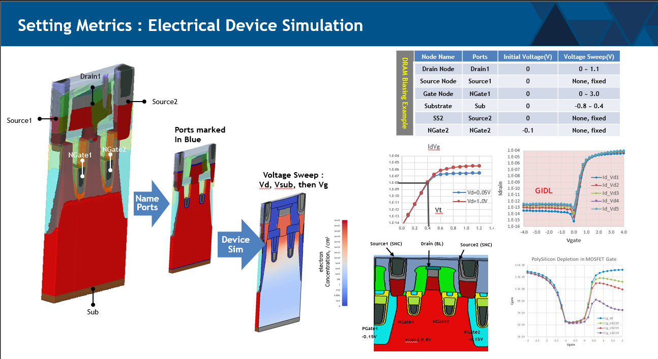
Traditional Design of Experiments (DOEs) for DRAM process characterization and optimization require significant off-process time and wafer costs, and are unacceptably lengthy and expensive. In this study, SEMulator3D is used to model the effect of etch tool variations (such as material selectivity or flux distribution) on device electrical performance. A simple DRAM device study is used to highlight the effect of gate etch behavior and etch step characteristics on electrical performance and yield targets, and to demonstrate how virtual fabrication can efficiently solve complex semiconductor manufacturing and yield challenges during DRAM technology development.
You might also be interested in:
- You must have an account on our Customer Portal to access this content. If you already have an account, please log in using the form below or to the right. […]
- You must have an account on our Customer Portal to access this content. If you already have an account, please log in using the form below or to the right. […]
- You must have an account on our Customer Portal to access this content. If you already have an account, please log in using the form below or to the right. […]
- You must have an account on our Customer Portal to access this content. If you already have an account, please log in using the form below or to the right. […]
- You must have an account on our Customer Portal to access this content. If you already have an account, please log in using the form below or to the right. […]
- You must have an account on our Customer Portal to access this content. If you already have an account, please log in using the form below or to the right. […]

