Skip to main content
LOG IN
REGISTER
Home
Customer Portal
Coventor Licensing Downloads
SEMulator3D Downloads
CoventorMP Downloads
Webinars
MEMS+ Courses
System Requirements
Software Licensing
Contact Us
✕
Enter your search
(more…)
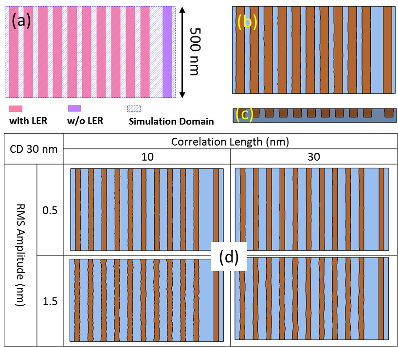
A Study of the Impact of Line Edge Roughness on Metal Line Resistance using Virtual Fabrication
Read more
- A Study of the Impact of Line Edge Roughness on Metal Line Resistance using Virtual Fabrication
A Study of the Impact of Line Edge Roughness on Metal Line Resistance using Virtual Fabrication
(more…)
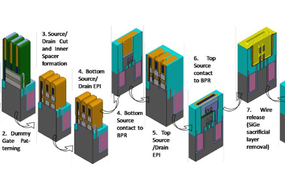
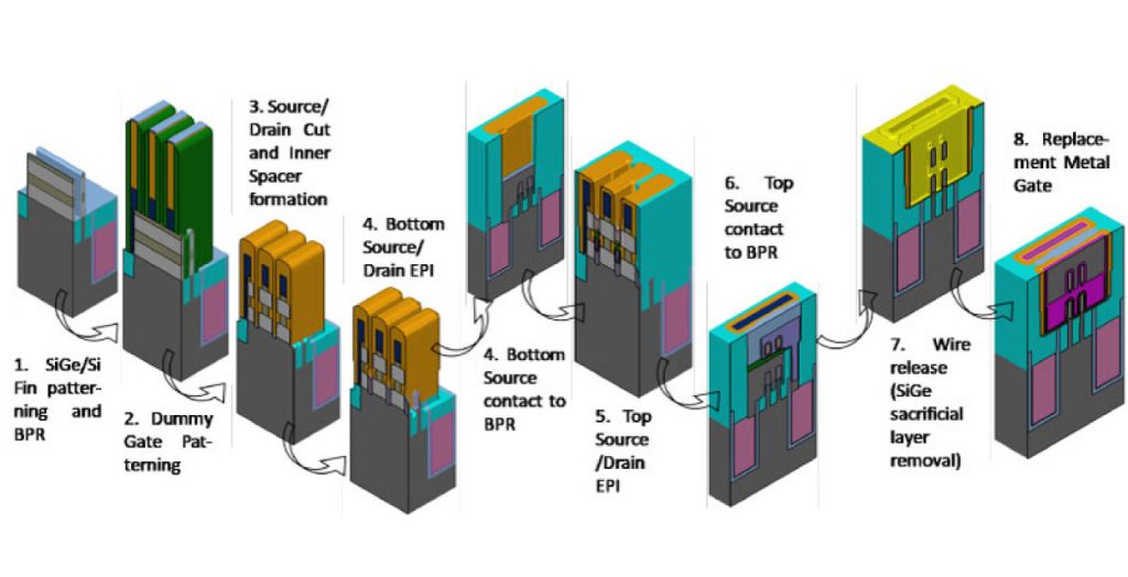
A Benchmark Study of Complementary-Field Effect Transistor (CFET) Process Integration Options: Comparing Bulk vs. SOI vs. DSOI Starting Substrates
Read more
- A Benchmark Study of Complementary-Field Effect Transistor (CFET) Process Integration Options: Comparing Bulk vs. SOI vs. DSOI Starting Substrates
A Benchmark Study of Complementary-Field Effect Transistor (CFET) Process Integration Options: Comparing Bulk vs. SOI vs. DSOI Starting Substrates
(more…)
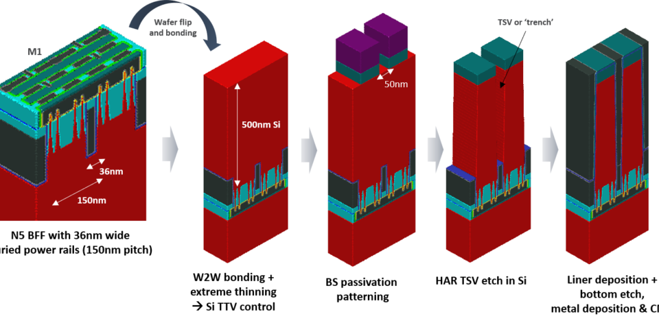
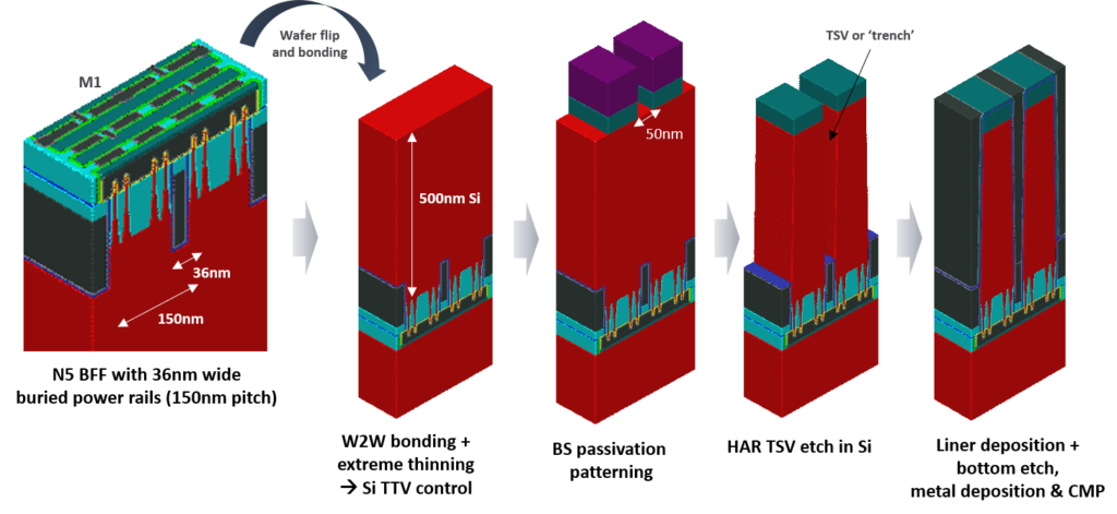
Backside Power Delivery as a Scaling Knob for Future Systems
Read more
- Backside Power Delivery as a Scaling Knob for Future Systems
Backside Power Delivery as a Scaling Knob for Future Systems
(more…)
Virtual Fabrication and Advanced Process Control Improve Yield for SAQP Process Assessment with 16 nm Half-Pitch
Read more
- Virtual Fabrication and Advanced Process Control Improve Yield for SAQP Process Assessment with 16 nm Half-Pitch
Virtual Fabrication and Advanced Process Control Improve Yield for SAQP Process Assessment with 16 nm Half-Pitch
(more…)
CMOS Area Scaling and the Need for High Aspect Ratio Vias
Read more
- CMOS Area Scaling and the Need for High Aspect Ratio Vias
CMOS Area Scaling and the Need for High Aspect Ratio Vias
(more…)
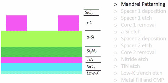
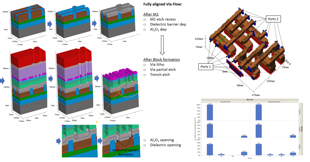
Self-Aligned Block and Fully Self-Aligned Via for iN5 Metal 2 Self-Aligned Quadruple Patterning
Read more
- Self-Aligned Block and Fully Self-Aligned Via for iN5 Metal 2 Self-Aligned Quadruple Patterning
Self-Aligned Block and Fully Self-Aligned Via for iN5 Metal 2 Self-Aligned Quadruple Patterning
(more…)
Modeling of Tone Inversion Process Flow for N5 Interconnect to Characterize Block Tip to Tip
Read more
- Modeling of Tone Inversion Process Flow for N5 Interconnect to Characterize Block Tip to Tip
Modeling of Tone Inversion Process Flow for N5 Interconnect to Characterize Block Tip to Tip
(more…)
Understanding how small variations in photoresist shape significantly impact multi-patterning yield
Read more
- Understanding how small variations in photoresist shape significantly impact multi-patterning yield
Understanding how small variations in photoresist shape significantly impact multi-patterning yield
(more…)
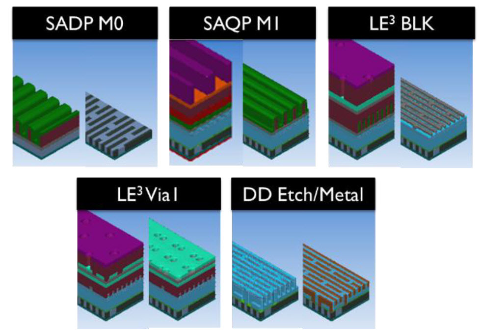
A million wafer, virtual fabrication approach to determine process capability requirements for an industry-standard N5 BEOL two-level metal flow
Read more
- A million wafer, virtual fabrication approach to determine process capability requirements for an industry-standard N5 BEOL two-level metal flow
A million wafer, virtual fabrication approach to determine process capability requirements for an industry-standard N5 BEOL two-level metal flow
(more…)
Load more
Contact Us
LOG IN
REGISTER
