Skip to main content
LOG IN
REGISTER
Home
Customer Portal
Coventor Licensing Downloads
SEMulator3D Downloads
CoventorMP Downloads
Webinars
MEMS+ Courses
System Requirements
Software Licensing
Contact Us
✕
Enter your search
(more…)
Pathfinding by process window modeling: Advanced DRAM capacitor patterning process window evaluation using virtual fabrication
Read more
- Pathfinding by process window modeling: Advanced DRAM capacitor patterning process window evaluation using virtual fabrication
Pathfinding by process window modeling: Advanced DRAM capacitor patterning process window evaluation using virtual fabrication
(more…)
A Study of the Impact of Line Edge Roughness on Metal Line Resistance using Virtual Fabrication
Read more
- A Study of the Impact of Line Edge Roughness on Metal Line Resistance using Virtual Fabrication
A Study of the Impact of Line Edge Roughness on Metal Line Resistance using Virtual Fabrication
(more…)
Evaluating the Impact of STI Recess Profile Control on Advanced FinFET Device Performance
Read more
- Evaluating the Impact of STI Recess Profile Control on Advanced FinFET Device Performance
Evaluating the Impact of STI Recess Profile Control on Advanced FinFET Device Performance
(more…)
The Effects of Poly Corner Etch Residue on Advanced FinFET Device Performance
Read more
- The Effects of Poly Corner Etch Residue on Advanced FinFET Device Performance
The Effects of Poly Corner Etch Residue on Advanced FinFET Device Performance
(more…)
SVT (six stacked vertical transistors) SRAM cell architecture introduction: design and process challenges assessment
Read more
- SVT (six stacked vertical transistors) SRAM cell architecture introduction: design and process challenges assessment
SVT (six stacked vertical transistors) SRAM cell architecture introduction: design and process challenges assessment
(more…)
A Triple-Deck CFET Structure with an Integrated SRAM Cell for the 2nm Technology Node and Beyond
Read more
- A Triple-Deck CFET Structure with an Integrated SRAM Cell for the 2nm Technology Node and Beyond
A Triple-Deck CFET Structure with an Integrated SRAM Cell for the 2nm Technology Node and Beyond
(more…)
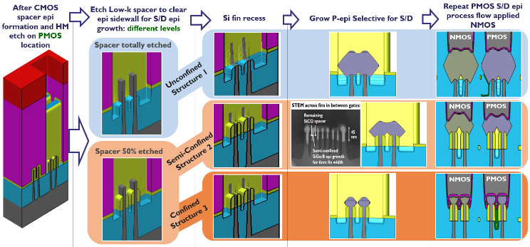
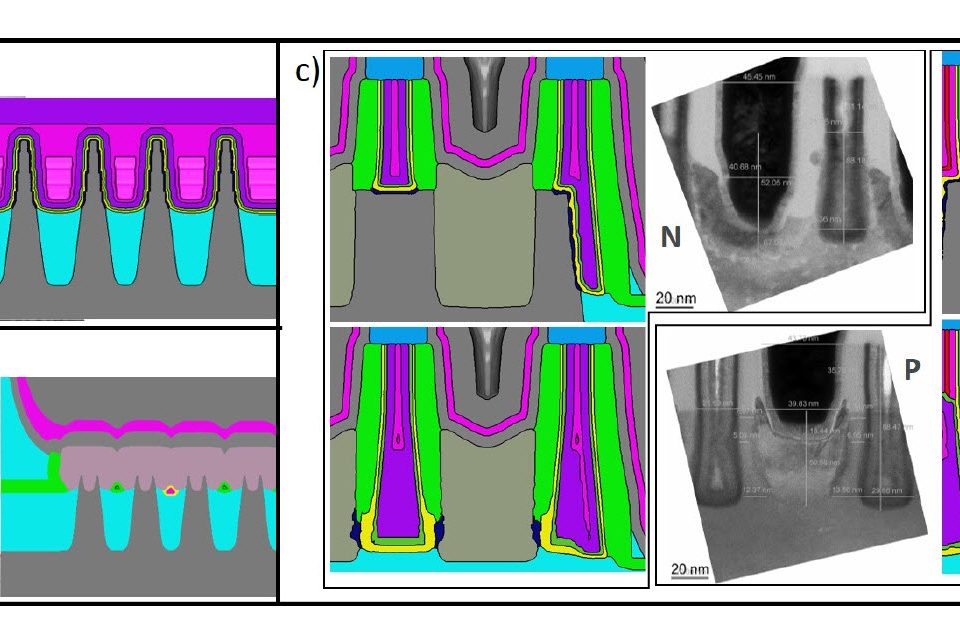
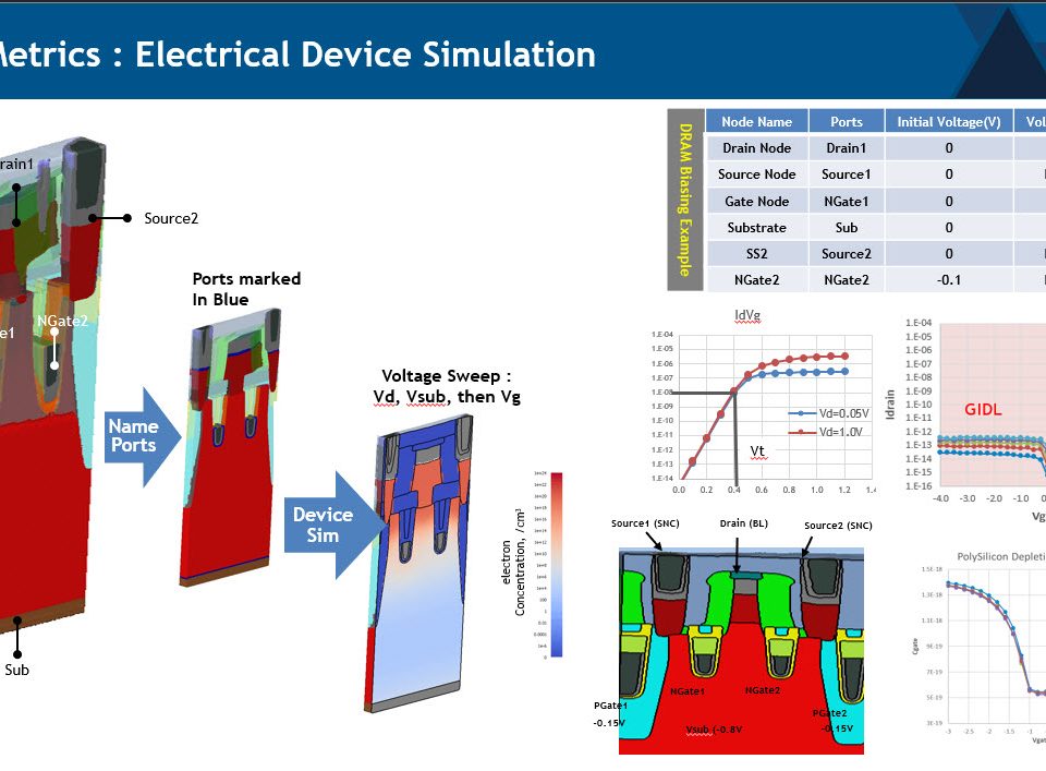
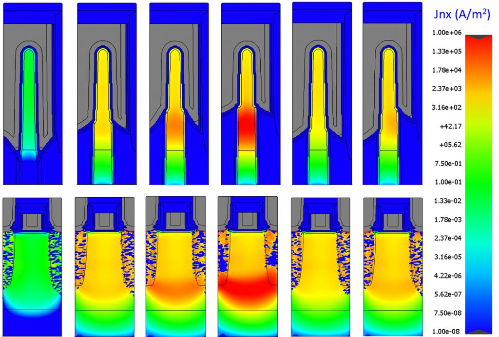
Evaluation of the impact of source drain epi implementation on logic performance using combined process and circuit simulation
Read more
- Evaluation of the impact of source drain epi implementation on logic performance using combined process and circuit simulation
Evaluation of the impact of source drain epi implementation on logic performance using combined process and circuit simulation
(more…)
Process Variation Analysis of Device Performance Using Virtual Fabrication: Methodology Demonstrated on a CMOS 14-nm FinFET Vehicle
Read more
- Process Variation Analysis of Device Performance Using Virtual Fabrication: Methodology Demonstrated on a CMOS 14-nm FinFET Vehicle
Process Variation Analysis of Device Performance Using Virtual Fabrication: Methodology Demonstrated on a CMOS 14-nm FinFET Vehicle
(more…)
Process Window Optimization of DRAM by Virtual Fabrication
Read more
- Process Window Optimization of DRAM by Virtual Fabrication
Process Window Optimization of DRAM by Virtual Fabrication
(more…)
Load more
Contact Us
LOG IN
REGISTER

