
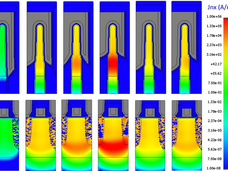
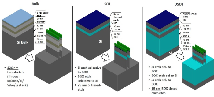
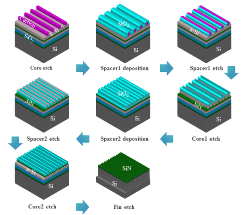
A Benchmark Study of Complementary-Field Effect Transistor (CFET) Process Integration Options: Comparing Bulk vs. SOI vs. DSOI Starting Substrates
November 15, 2019You must have an account on our Customer Portal to access this content. If you already have an account, please log in using the form below or to the right. If you do not have an account, we invite you to request an account.
Whitepaper: Everything You Need to Know about FDSOI Technology – Advantages, Disadvantages, and Applications of FDSOI

To download your free white paper, please fill out the form below:
Over the past decades, transistor feature size has continuously decreased, leading to an increase in performance and a reduction in power consumption. Consumers have reaped the benefits, with superior electronic devices that have become increasingly useful, valuable, faster and more efficient. In recent years, as transistor feature size has shrunk below 10nm, it has become progressively more difficult to meet the many challenges of next generation technology. One such challenge involves leakage current, which now represents a significant proportion of transistor power consumption. The design of bulk-silicon transistors has become more complex, to keep leakage current under control. This design complexity has generated the need for additional manufacturing steps, and a move toward new and expensive 3D architectures. Semiconductor companies, such as ST Microelectronics, GlobalFoundries, Samsung and others, have introduced new innovations in silicon process technology to lower design complexity, reduce power requirements, and incrementally leverage their existing manufacturing capabilities.
Fully Depleted Silicon on Insulator, or FDSOI, is a planar process technology that delivers the benefits of reduced silicon geometries while simplifying the manufacturing process. This process technology relies on two primary innovations. First, an ultra-thin layer of insulator, called the buried oxide, is positioned on top of the base silicon. Then, a very thin silicon film is used to form a transistor channel. Due to the thin film silicon structure, there is no need to dope the channel, thus making the transistor “fully depleted”. The combination of these two innovations is called “Ultra-Thin Body and Buried oxide Fully Depleted SOI” or UTBB-FDSOI. In this paper, we will first describe SOI (Silicon on Insulator) wafers and their characteristics. We will then discuss FDSOI technology, including the main benefits of this technology, differentiation with FinFET technology, and key applications.
You might also be interested in:
- You must have an account on our Customer Portal to access this content. If you already have an account, please log in using the form below or to the right. […]
- You must have an account on our Customer Portal to access this content. If you already have an account, please log in using the form below or to the right. […]
- You must have an account on our Customer Portal to access this content. If you already have an account, please log in using the form below or to the right. […]
- You must have an account on our Customer Portal to access this content. If you already have an account, please log in using the form below or to the right. […]
- You must have an account on our Customer Portal to access this content. If you already have an account, please log in using the form below or to the right. […]
- You must have an account on our Customer Portal to access this content. If you already have an account, please log in using the form below or to the right. […]
- You must have an account on our Customer Portal to access this content. If you already have an account, please log in using the form below or to the right. […]
- You must have an account on our Customer Portal to access this content. If you already have an account, please log in using the form below or to the right. […]
- You must have an account on our Customer Portal to access this content. If you already have an account, please log in using the form below or to the right. […]
- You must have an account on our Customer Portal to access this content. If you already have an account, please log in using the form below or to the right. […]
- You must have an account on our Customer Portal to access this content. If you already have an account, please log in using the form below or to the right. […]
- You must have an account on our Customer Portal to access this content. If you already have an account, please log in using the form below or to the right. […]

