Skip to main content
LOG IN
REGISTER
Home
Customer Portal
Coventor Licensing Downloads
SEMulator3D Downloads
CoventorMP Downloads
Webinars
MEMS+ Courses
System Requirements
Software Licensing
Contact Us
✕
Enter your search
(more…)
Evaluating the Impact of STI Recess Profile Control on Advanced FinFET Device Performance
Read more
- Evaluating the Impact of STI Recess Profile Control on Advanced FinFET Device Performance
Evaluating the Impact of STI Recess Profile Control on Advanced FinFET Device Performance
(more…)
The Effects of Poly Corner Etch Residue on Advanced FinFET Device Performance
Read more
- The Effects of Poly Corner Etch Residue on Advanced FinFET Device Performance
The Effects of Poly Corner Etch Residue on Advanced FinFET Device Performance
(more…)
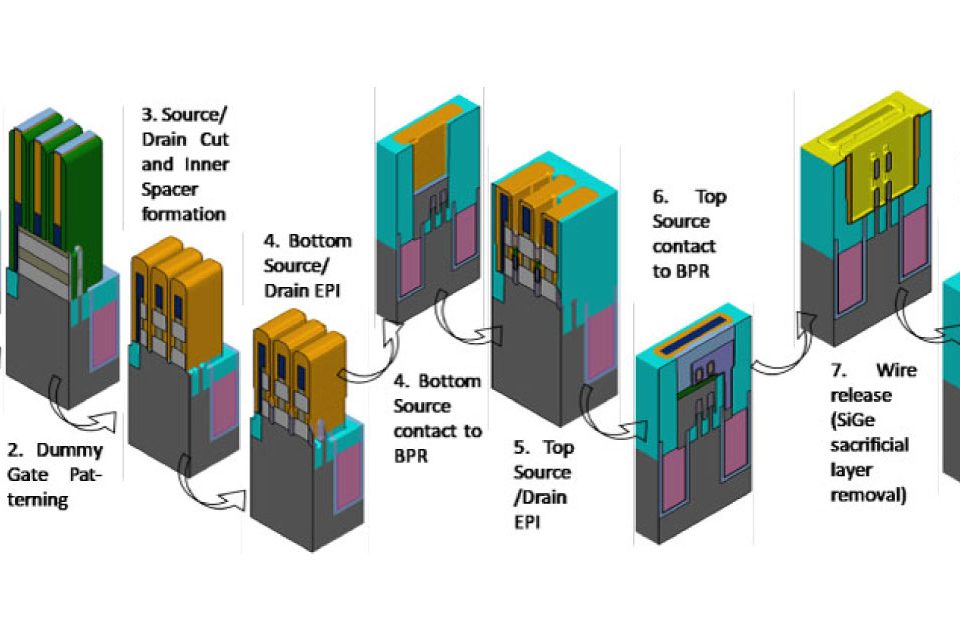
A Triple-Deck CFET Structure with an Integrated SRAM Cell for the 2nm Technology Node and Beyond
Read more
- A Triple-Deck CFET Structure with an Integrated SRAM Cell for the 2nm Technology Node and Beyond
A Triple-Deck CFET Structure with an Integrated SRAM Cell for the 2nm Technology Node and Beyond
(more…)
Evaluation of the impact of source drain epi implementation on logic performance using combined process and circuit simulation
Read more
- Evaluation of the impact of source drain epi implementation on logic performance using combined process and circuit simulation
Evaluation of the impact of source drain epi implementation on logic performance using combined process and circuit simulation
(more…)
Process Variation Analysis of Device Performance Using Virtual Fabrication: Methodology Demonstrated on a CMOS 14-nm FinFET Vehicle
Read more
- Process Variation Analysis of Device Performance Using Virtual Fabrication: Methodology Demonstrated on a CMOS 14-nm FinFET Vehicle
Process Variation Analysis of Device Performance Using Virtual Fabrication: Methodology Demonstrated on a CMOS 14-nm FinFET Vehicle
(more…)
Process Model Calibration: The Key to Building Predictive and Accurate 3D Process Models
Read more
- Process Model Calibration: The Key to Building Predictive and Accurate 3D Process Models
Process Model Calibration: The Key to Building Predictive and Accurate 3D Process Models
(more…)
A Benchmark Study of Complementary-Field Effect Transistor (CFET) Process Integration Options done by Virtual Fabrication
Read more
- A Benchmark Study of Complementary-Field Effect Transistor (CFET) Process Integration Options done by Virtual Fabrication
A Benchmark Study of Complementary-Field Effect Transistor (CFET) Process Integration Options done by Virtual Fabrication
(more…)
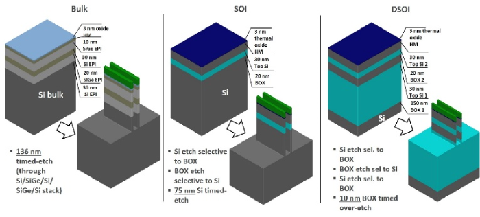
A Benchmark Study of Complementary-Field Effect Transistor (CFET) Process Integration Options: Comparing Bulk vs. SOI vs. DSOI Starting Substrates
Read more
- A Benchmark Study of Complementary-Field Effect Transistor (CFET) Process Integration Options: Comparing Bulk vs. SOI vs. DSOI Starting Substrates
A Benchmark Study of Complementary-Field Effect Transistor (CFET) Process Integration Options: Comparing Bulk vs. SOI vs. DSOI Starting Substrates
(more…)
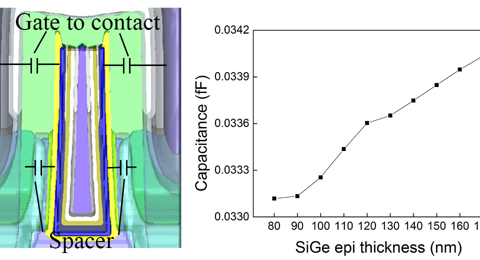
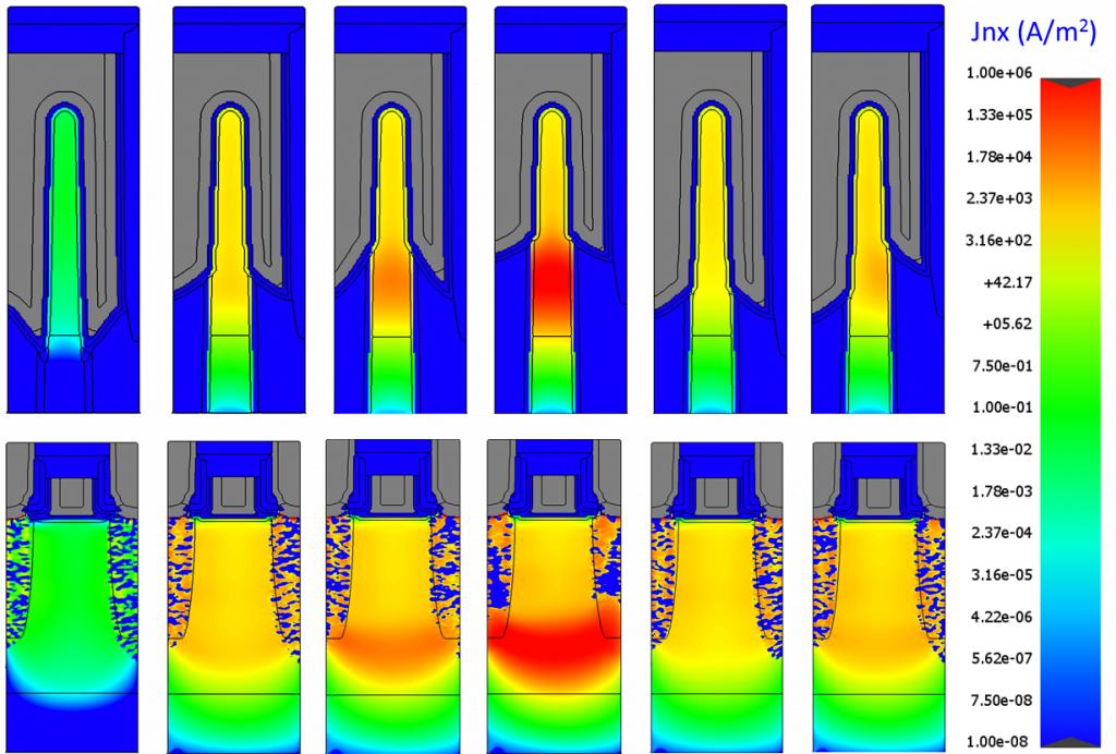
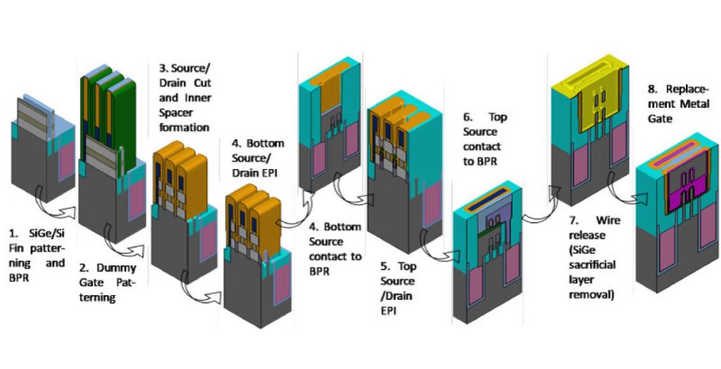
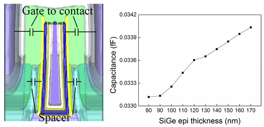
Influence of SiGe on Parasitic Parameters in PMOS
Read more
- Influence of SiGe on Parasitic Parameters in PMOS
Influence of SiGe on Parasitic Parameters in PMOS
(more…)
Load more
Contact Us
LOG IN
REGISTER

