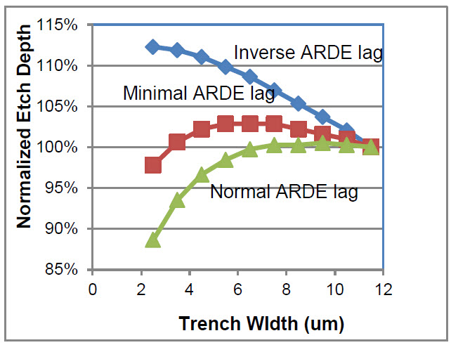
New Techniques to Analyze and Reduce Etch Variation
January 20, 2017
Understanding how small variations in photoresist shape significantly impact multi-patterning yield
April 12, 2017You must have an account on our Customer Portal to access this content. If you already have an account, please log in using the form below or to the right. If you do not have an account, we invite you to request an account.
Whitepaper: Optimizing DRAM Development using Directed Self-Assembly (DSA)

To download your free white paper, please fill out the form below:
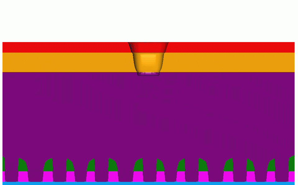
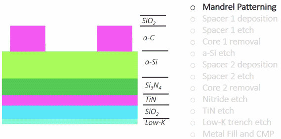
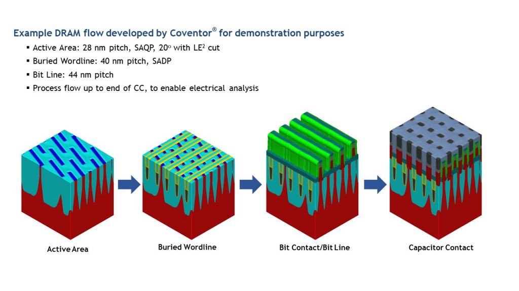
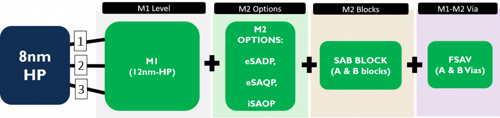
Directed Self-Assembly (DSA) is an emerging technology that has the ability to substantially improve lithographic manufacturing of semiconductor devices. In DSA, copolymer materials self-assemble to form nanoscale resolution patterns on the semiconductor substrate. DSA technologies hold the promise to substantially improve the resolution of existing lithographic processes (such as self-aligned quadruple patterning, or SAQP), leading to higher density semiconductor devices.
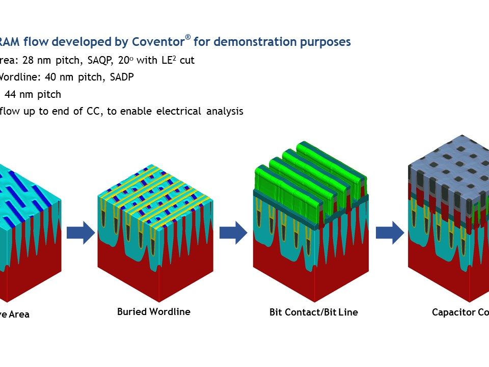
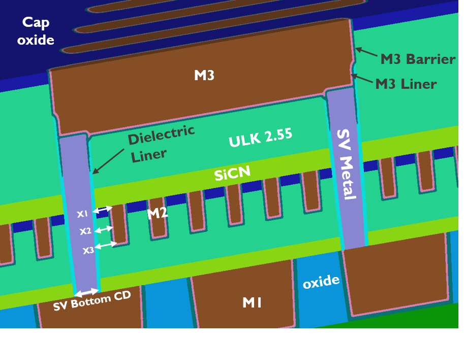
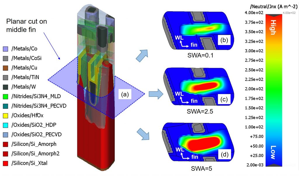
SEMulator3D can be used to model potential issues with the adoption of new and advanced DRAM patterning and lithography technologies such as DSA. We can use SEMulator3D to study the effect of Directed Self-Assembly (DSA) during semiconductor manufacturing. In this study, we examine how the incorporation of advanced DSA patterning processes might affect the fabrication of a 14-nm DRAM array. A behavioral DSA process model was used to replace SAQP with DSA during active area patterning, including the replacement of LE4 by DSA for the hexagonally packed DRAM capacitors. We quantified the impact of the SAQP module replacement by looking at a key process yield metric for DRAM, the interface area between the capacitor contacts and transistor source/drain.
Mattan Kamon, Mustafa Akbulut, Yiguang Yan, Daniel Faken, Andras Pap, Vasanth Allampalli, Ken Greiner, David Fried, “Virtual fabrication using directed self-assembly for process optimization in a 14-nm dynamic random access memory,” J. Micro/Nanolith. MEMS MOEMS 15(3), 031605 (2016)
http://dx.doi.org/10.1117/1.JMM.15.3.031605
Copyright 2016 Society of Photo Optical Instrumentation Engineers. One print or electronic copy may be made for personal use only. Systematic reproduction and distribution, duplication of any material in this paper for a fee or for commercial purposes, or modification of the content of the paper are prohibited.
You might also be interested in:
- You must have an account on our Customer Portal to access this content. If you already have an account, please log in using the form below or to the right. […]
- You must have an account on our Customer Portal to access this content. If you already have an account, please log in using the form below or to the right. […]
- You must have an account on our Customer Portal to access this content. If you already have an account, please log in using the form below or to the right. […]
- You must have an account on our Customer Portal to access this content. If you already have an account, please log in using the form below or to the right. […]
- You must have an account on our Customer Portal to access this content. If you already have an account, please log in using the form below or to the right. […]
Impact of EUV Resist Thickness on Local Critical Dimension Uniformities for <30 nm CD Via Patterning
Impact of EUV Resist Thickness on Local Critical Dimension Uniformities for <30 nm CD Via Patterning
You must have an account on our Customer Portal to access this content. If you already have an account, please log in using the form below or to the right. […]- You must have an account on our Customer Portal to access this content. If you already have an account, please log in using the form below or to the right. […]
- You must have an account on our Customer Portal to access this content. If you already have an account, please log in using the form below or to the right. […]
- You must have an account on our Customer Portal to access this content. If you already have an account, please log in using the form below or to the right. […]
- You must have an account on our Customer Portal to access this content. If you already have an account, please log in using the form below or to the right. […]
- You must have an account on our Customer Portal to access this content. If you already have an account, please log in using the form below or to the right. […]
- You must have an account on our Customer Portal to access this content. If you already have an account, please log in using the form below or to the right. […]

