![3D NAND flash memory array, based on TCAT [1], with 16 cells per string, top gate-select layer and bottom source-select layer.](https://www.coventor.com/wp-content/uploads/2014/05/TCAT_whole_bf-M1-marked1.png)
3D NAND Flash Processing
March 10, 2015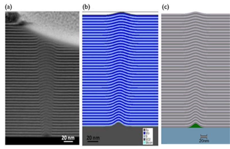
Defect Evolution in Next Generation, Extreme Ultraviolet Lithography
February 20, 2016You must have an account on our Customer Portal to access this content. If you already have an account, please log in using the form below or to the right. If you do not have an account, we invite you to request an account.
Whitepaper: Modeling of Cross Wafer Induced Process Variations

To download your free white paper, please fill out the form below:
3D semiconductors, 3D NAND Flash, FinFETS and other advanced devices are bringing tremendous opportunities to the semiconductor industry. Unfortunately, these devices are also bringing new design, process and production problems. Process variability has been a major contributor to production delays as feature sizes have decreased and process complexity has increased.
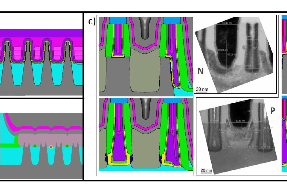
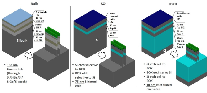
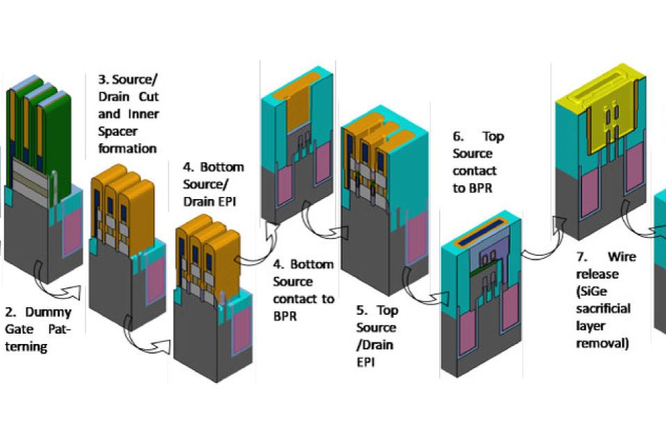
Virtual fabrication is a computerized technique to perform predictive, three dimensional modeling of semiconductor fabrication processes. Virtual fabrication allows engineers to test semiconductor process changes and process variability in minutes or hours, instead of the weeks or months required to test their designs using actual semiconductor wafers.
This white paper explores the modeling of cross wafer die-to-die semiconductor process variations using virtual fabrication techniques available in SEMulator3D.
You might also be interested in:
- You must have an account on our Customer Portal to access this content. If you already have an account, please log in using the form below or to the right. […]
- You must have an account on our Customer Portal to access this content. If you already have an account, please log in using the form below or to the right. […]
- You must have an account on our Customer Portal to access this content. If you already have an account, please log in using the form below or to the right. […]
- You must have an account on our Customer Portal to access this content. If you already have an account, please log in using the form below or to the right. […]
- You must have an account on our Customer Portal to access this content. If you already have an account, please log in using the form below or to the right. […]
- You must have an account on our Customer Portal to access this content. If you already have an account, please log in using the form below or to the right. […]
- You must have an account on our Customer Portal to access this content. If you already have an account, please log in using the form below or to the right. […]
- You must have an account on our Customer Portal to access this content. If you already have an account, please log in using the form below or to the right. […]
- You must have an account on our Customer Portal to access this content. If you already have an account, please log in using the form below or to the right. […]
- You must have an account on our Customer Portal to access this content. If you already have an account, please log in using the form below or to the right. […]
- You must have an account on our Customer Portal to access this content. If you already have an account, please log in using the form below or to the right. […]

