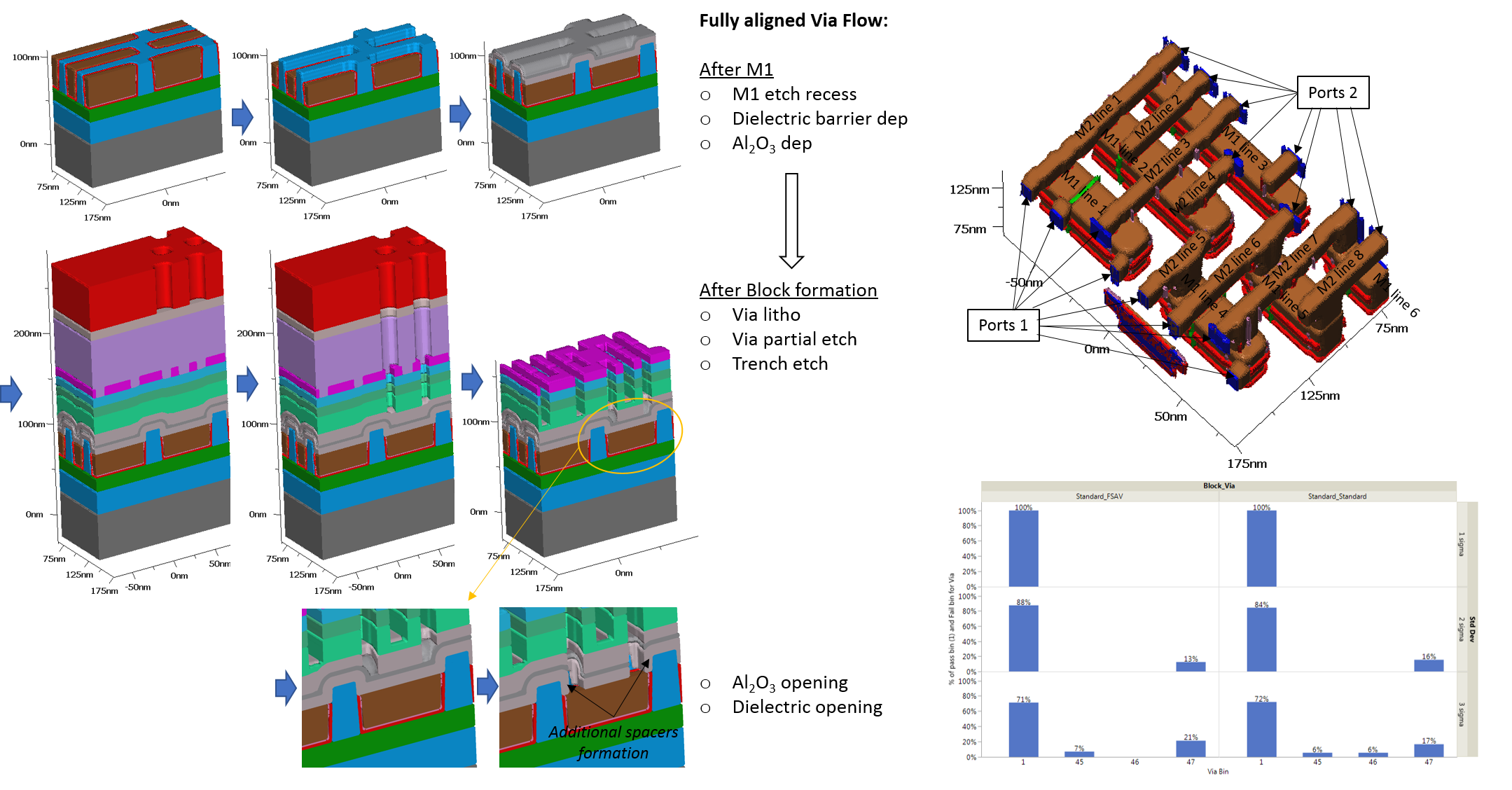
Self-Aligned Block and Fully Self-Aligned Via for iN5 Metal 2 Self-Aligned Quadruple Patterning
March 14, 2018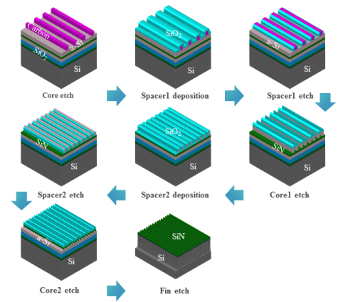
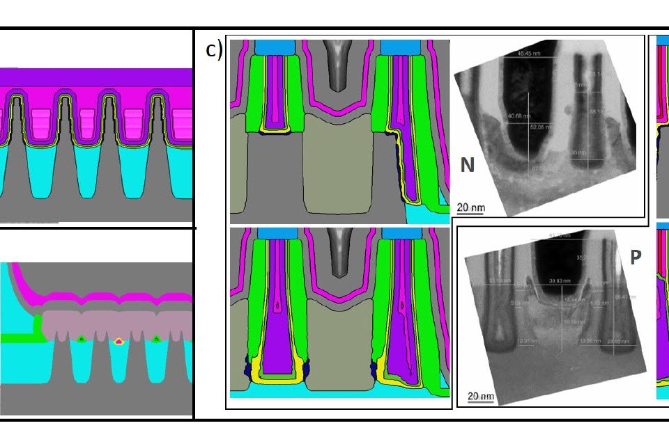
N7 FinFET Self-Aligned Quadruple Patterning Modeling
July 19, 2018You must have an account on our Customer Portal to access this content. If you already have an account, please log in using the form below or to the right. If you do not have an account, we invite you to request an account.
Whitepaper: Understanding the Effect of Variability in Bulk FinFET Device Performance

To download your free white paper, please fill out the form below:
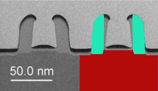
2-D MOSFETs have proven difficult to scale down to 20nm and beyond. In their place, 3D FinFET transistors have emerged as novel devices that can scale down to lower node sizes. . 10nm process FinFETs are for SoC product mass production, and research is progressing towards a 7nm process FinFET. FinFET transistors provide lower dynamic power consumption (due to flatter I-V curves), improved control over short channel effects, a reduction of leakage current, superior on/off contrast, and most importantly, less wafer area per transistor than 2-D MOSFET technology.
Unfortunately, the transition from planar to FinFET technology has come with new sources of variability inherent in 3D device geometry. 3D device simulation can be a very useful tool to investigate the impact of this variability on device performance. 3D simulation is widely used to analyze and optimize MOSFET characteristics such as threshold voltage, on / off current, sub-threshold swing and drain-induced barrier lowering due to changes in fin geometry, doping concentration, and other 3D device geometry variations. Furthermore, the effects of random fluctuations in process distribution and roughness can be explored using semiconductor process simulation platforms such as SEMulator3D®.
You might also be interested in:
- You must have an account on our Customer Portal to access this content. If you already have an account, please log in using the form below or to the right. […]
- You must have an account on our Customer Portal to access this content. If you already have an account, please log in using the form below or to the right. […]
- You must have an account on our Customer Portal to access this content. If you already have an account, please log in using the form below or to the right. […]
- You must have an account on our Customer Portal to access this content. If you already have an account, please log in using the form below or to the right. […]
- You must have an account on our Customer Portal to access this content. If you already have an account, please log in using the form below or to the right. […]
- You must have an account on our Customer Portal to access this content. If you already have an account, please log in using the form below or to the right. […]
- You must have an account on our Customer Portal to access this content. If you already have an account, please log in using the form below or to the right. […]
Impact of EUV Resist Thickness on Local Critical Dimension Uniformities for <30 nm CD Via Patterning
Impact of EUV Resist Thickness on Local Critical Dimension Uniformities for <30 nm CD Via Patterning
You must have an account on our Customer Portal to access this content. If you already have an account, please log in using the form below or to the right. […]- You must have an account on our Customer Portal to access this content. If you already have an account, please log in using the form below or to the right. […]
- You must have an account on our Customer Portal to access this content. If you already have an account, please log in using the form below or to the right. […]
- You must have an account on our Customer Portal to access this content. If you already have an account, please log in using the form below or to the right. […]
- You must have an account on our Customer Portal to access this content. If you already have an account, please log in using the form below or to the right. […]

