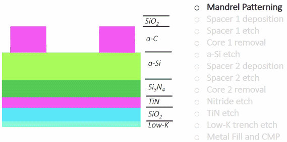
Virtual Fabrication and Advanced Process Control Improve Yield for SAQP Process Assessment with 16 nm Half-Pitch
March 21, 2019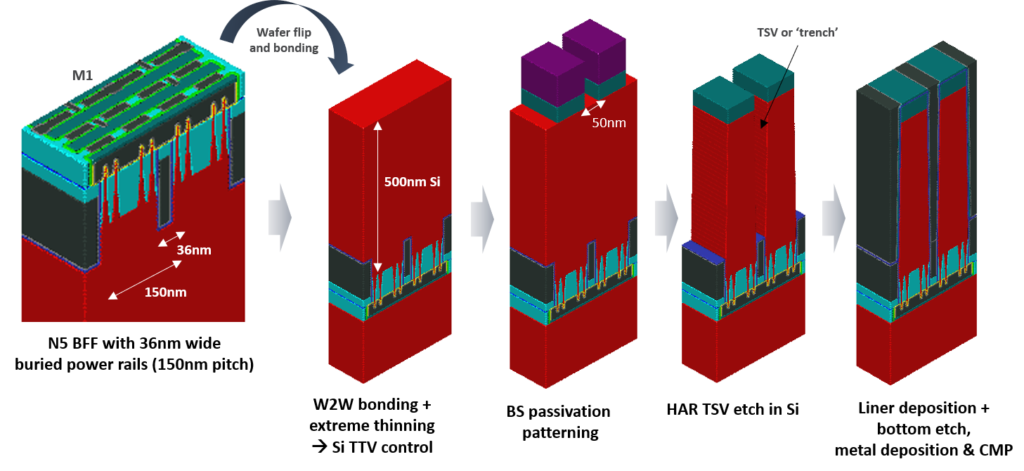
Backside Power Delivery as a Scaling Knob for Future Systems
July 3, 2019You must have an account on our Customer Portal to access this content. If you already have an account, please log in using the form below or to the right. If you do not have an account, we invite you to request an account.
Whitepaper: Self-aligned Fin Cut Last Patterning Scheme for Fin Arrays of 24nm Pitch and Beyond

To download your free white paper, please fill out the form below:
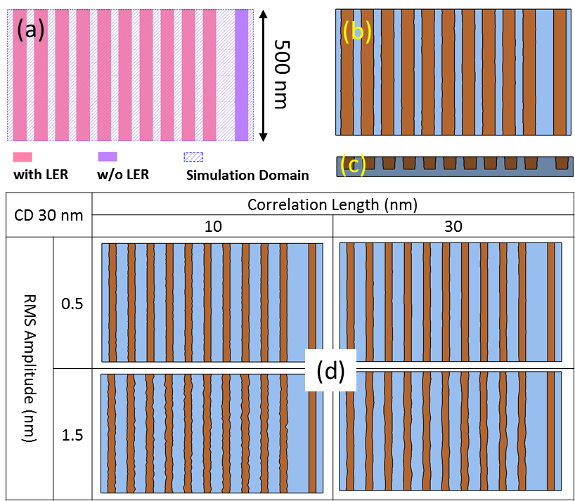
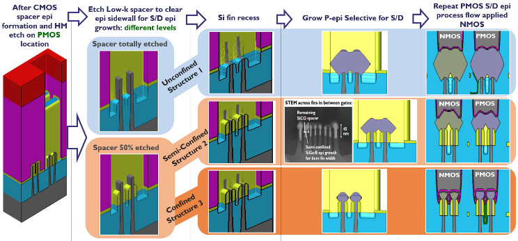
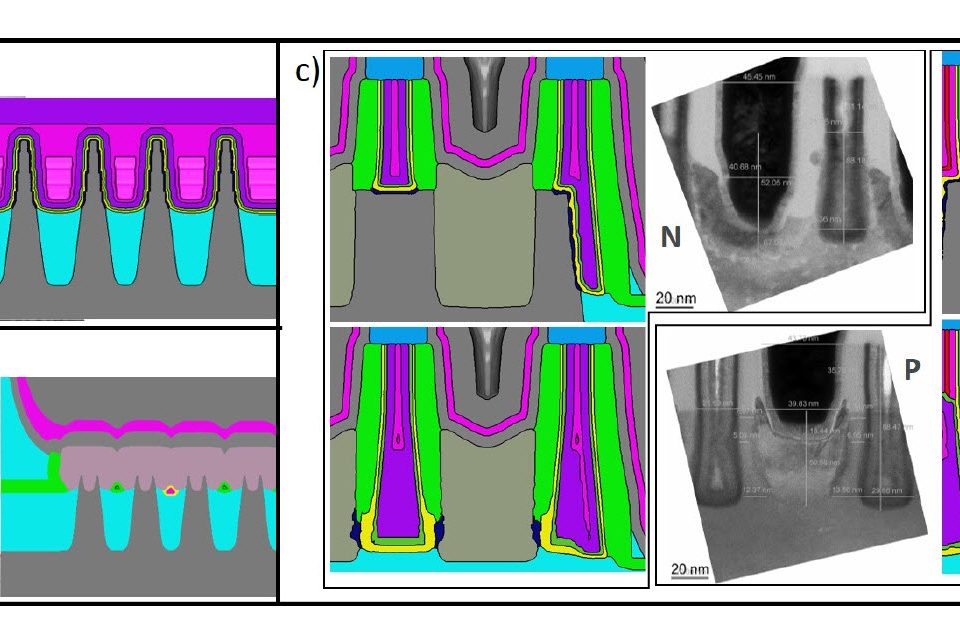
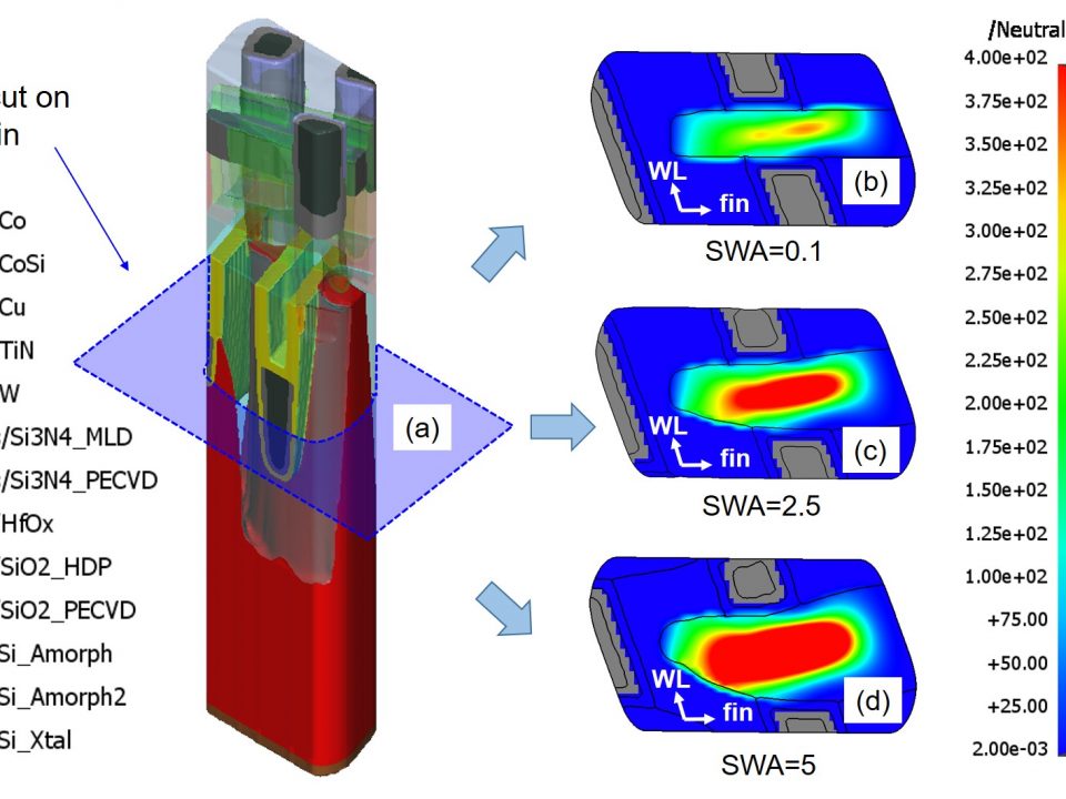
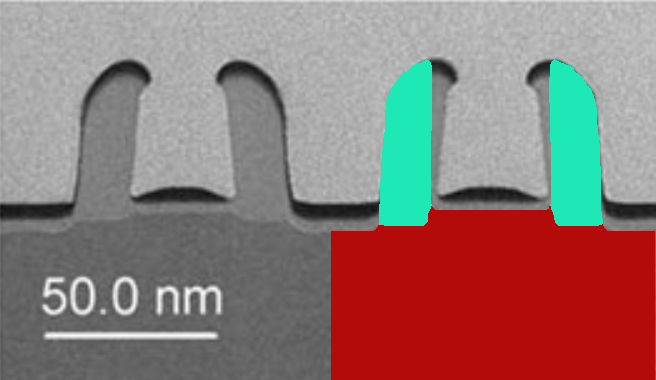
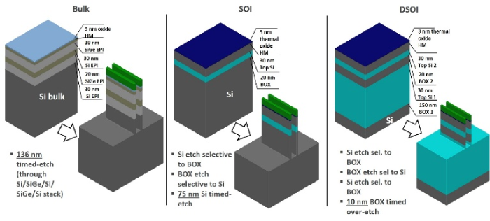
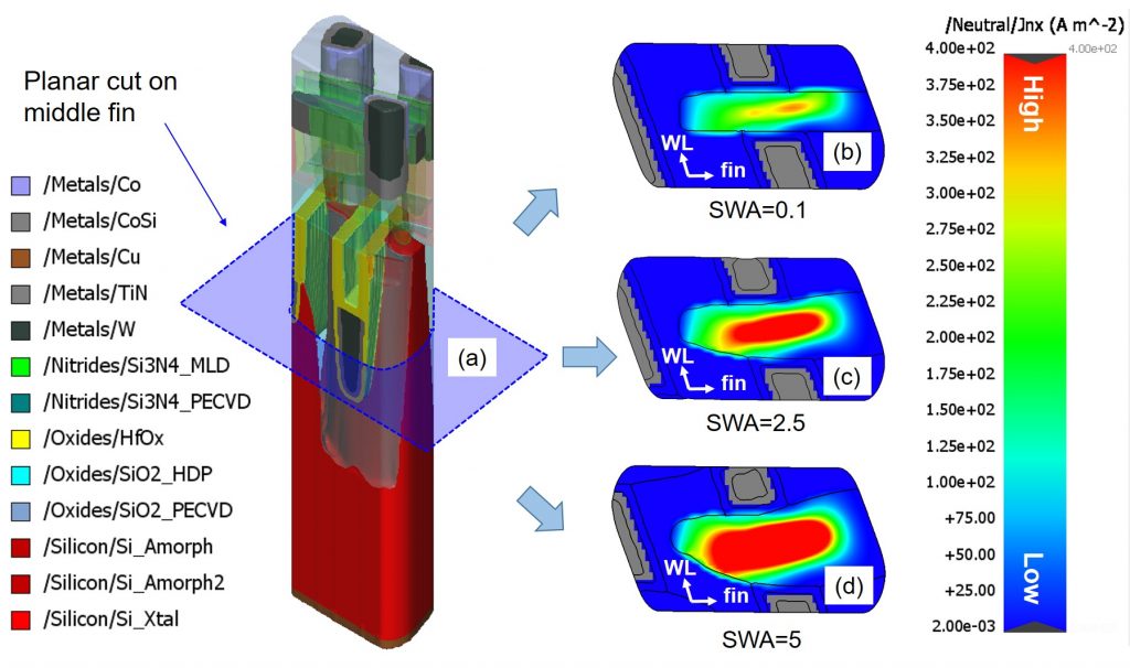
In 5 nm FinFET technology and beyond, SRAM cell size reduction to 6 tracks is required with a fin pitch of 24 nm. Fin depopulation is mandatory to enable area scaling, but it becomes challenging at small pitches. In the first part of our study, we simulate a FinFET process flow with various fin cut approaches to obtain a 3D model of a FinFET SRAM device. Layout dependent effects on silicon and process non-idealities are characterized in a second part and used to calibrate the 3D model. In the third part of our work, a process sensitivity analysis is performed to compare the impact of overlay and CD variations on various fin cut options.
© (2019) COPYRIGHT Society of Photo-Optical Instrumentation Engineers (SPIE). Downloading of the abstract is permitted for personal use only.
S. Baudot, A. Soussou, A. P. Milenin, T. Hopf, S. Wang, P. Weckx, B. Vincent, J. Ervin, and S. Demuynck, "Self-aligned fin cut last patterning scheme for fin arrays of 24nm pitch and beyond", Proc. SPIE 10960, Advances in Patterning Materials and Processes XXXVI, 109600N (25 March 2019); doi: 10.1117/12.2514927;
https://doi.org/10.1117/12.2514927
You might also be interested in:
- You must have an account on our Customer Portal to access this content. If you already have an account, please log in using the form below or to the right. […]
- You must have an account on our Customer Portal to access this content. If you already have an account, please log in using the form below or to the right. […]
- You must have an account on our Customer Portal to access this content. If you already have an account, please log in using the form below or to the right. […]
- You must have an account on our Customer Portal to access this content. If you already have an account, please log in using the form below or to the right. […]
- You must have an account on our Customer Portal to access this content. If you already have an account, please log in using the form below or to the right. […]
- You must have an account on our Customer Portal to access this content. If you already have an account, please log in using the form below or to the right. […]
- You must have an account on our Customer Portal to access this content. If you already have an account, please log in using the form below or to the right. […]
- You must have an account on our Customer Portal to access this content. If you already have an account, please log in using the form below or to the right. […]
- You must have an account on our Customer Portal to access this content. If you already have an account, please log in using the form below or to the right. […]
- You must have an account on our Customer Portal to access this content. If you already have an account, please log in using the form below or to the right. […]
Impact of EUV Resist Thickness on Local Critical Dimension Uniformities for <30 nm CD Via Patterning
Impact of EUV Resist Thickness on Local Critical Dimension Uniformities for <30 nm CD Via Patterning
You must have an account on our Customer Portal to access this content. If you already have an account, please log in using the form below or to the right. […]- You must have an account on our Customer Portal to access this content. If you already have an account, please log in using the form below or to the right. […]


