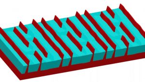
• Skip to main content
  • LOG IN
  • REGISTER
Coventor_New_LogoCoventor_New_LogoCoventor_New_LogoCoventor_New_Logo
  • COMPANY
    • ABOUT
    • CAREERS
    • PRESS RELEASE
    • PRESS COVERAGE
    • EVENTS
  • PRODUCTS
    • SEMulator3D®
      Semiconductor Process Modeling
    • CoventorMP®
      MEMS Design Automation
      • CoventorWare®
      • MEMS+®
  • SOLUTIONS
    • SEMICONDUCTOR SOLUTIONS
    • MEMS SOLUTIONS
  • RESOURCES
    • CASE STUDIES
    • BLOG
    • VIDEOS
  • CONTACT
  • SUPPORT
Contact Us
✕
  • Home
  • Mustafa Akbulut
  • Filter by
  • Categories
  • Tags
  • Authors
  • Show all
  • All
  • Coventor Blog
  • Press Releases
  • All
  • 3D DRAM
  • 3D NAND
  • ALD
  • AVS 68
  • BEOL
  • bulk Si
  • Capacitance Analysis
  • CFET
  • chip packaging
  • CMP
  • Coventor
  • CoventorMP
  • CoventorWare
  • Defect Analysis
  • Deposition
  • Digital Twins
  • DRAM
  • dry etch
  • DSOI
  • DTCO (Design Technology Co-Optimization)
  • EDTM 2023
  • Equipment Intelligence
  • Etch
  • EUV
  • Extreme Ultraviolet lithography
  • FEOL
  • FinFET
  • gyroscope
  • HVM
  • IEEE Inertial Sensors 2023
  • IEEE MEMS 2023
  • imec
  • ISS 2023
  • Line Edge Roughness (LER)
  • Lithography and Patterning
  • Machine Learning
  • MEMS
  • MEMS Accelerometer
  • MEMS gyroscope
  • MEMS Inertial Sensors
  • MEMS Micro Mirror
  • MEMS Microphone
  • MEMS PDK (Process Design Kits)
  • MEMS Pressure Sensor
  • MEMS RF Switch
  • MEMS Seismometer
  • MEMS Switch
  • MEMS+
  • mesh
  • Meshing
  • Nanosheet
  • NEMS
  • NEMS BEOL
  • Netlist
  • Netlisting
  • Piezoelectric MEMS
  • Process Library
  • Process Model Calibration
  • Process Window Optimization
  • SADP
  • SAQP
  • SEMI
  • SEMICON Korea 2023
  • Semiconductor Metrology
  • SEMulator3D
  • SEMulator3D; DRAM; FEOL
  • Silicon Photonics
  • SOI
  • SPIE Advanced Lithography 2023
  • SRAM
  • TCAD
  • Technology Review
  • Technology Reviews
  • Transducers 2023
  • All
  • Coventor
  • Arnaud Parent
  • Assawer Soussou
  • Brett Lowe
  • Benjamin Vincent
  • Chris Welham
  • Dempsey Deng
  • David Fried
  • Daebin Yim
  • Gerold Schropfer
  • Hideyuki Maekoba
  • Joan Asselot
  • Jacky Huang
  • Jeonghoon Kim
  • Kira Egelhofer Ruegger
  • Mustafa Akbulut
  • Mattan Kamon
  • Martha Lee
  • Pradeep Nanja
  • QingPeng Wang
  • Ryan Miller
  • Sumant Sarkar
  • Sandy Wen
  • Tae Yeon Oh
  • Timothy Yang
  • Vincent Huber
  • Yu De Chen
  • Brian Van Dyk
April 12, 2017
Published by Mustafa Akbulut at April 12, 2017
Categories
  • Coventor Blog

Photoresist shape in 3D: Understanding how small variations in photoresist shape significantly impact multi-patterning yield

Things were easy for integrators when the pattern they had on the mask ended up being the pattern they wanted on the chip. Multi-patterning schemes such as Self-Aligned Double Patterning […]
Do you like it?
Read more - Photoresist shape in 3D: Understanding how small variations in photoresist shape significantly impact multi-patterning yield

Product Information

  • Product Offerings
  • Technical Support & Training
  • Licensing
  • System Requirements

Resources

  • Blog
  • Case Studies
  • Videos
  • 2018 MEMS Design Contest

Company

  • About
  • Press
  • Partners & Programs
  • Contact
© Copyright Coventor Inc., A Lam Research Company, All Rights Reserved
Privacy Policy • Terms of Use
Contact Us
  • LOG IN
  • REGISTER