With continuous device scaling, process windows have become narrower and narrower due to smaller feature sizes and greater process step variability [1]. A key task during the R&D stage of […]
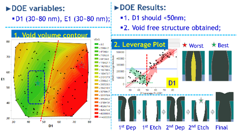
Design of Experiments (DOE) is a powerful concept in semiconductor engineering research and development. DOEs are sets of experiments used to explore the sensitivity of experimental variables and their effect […]
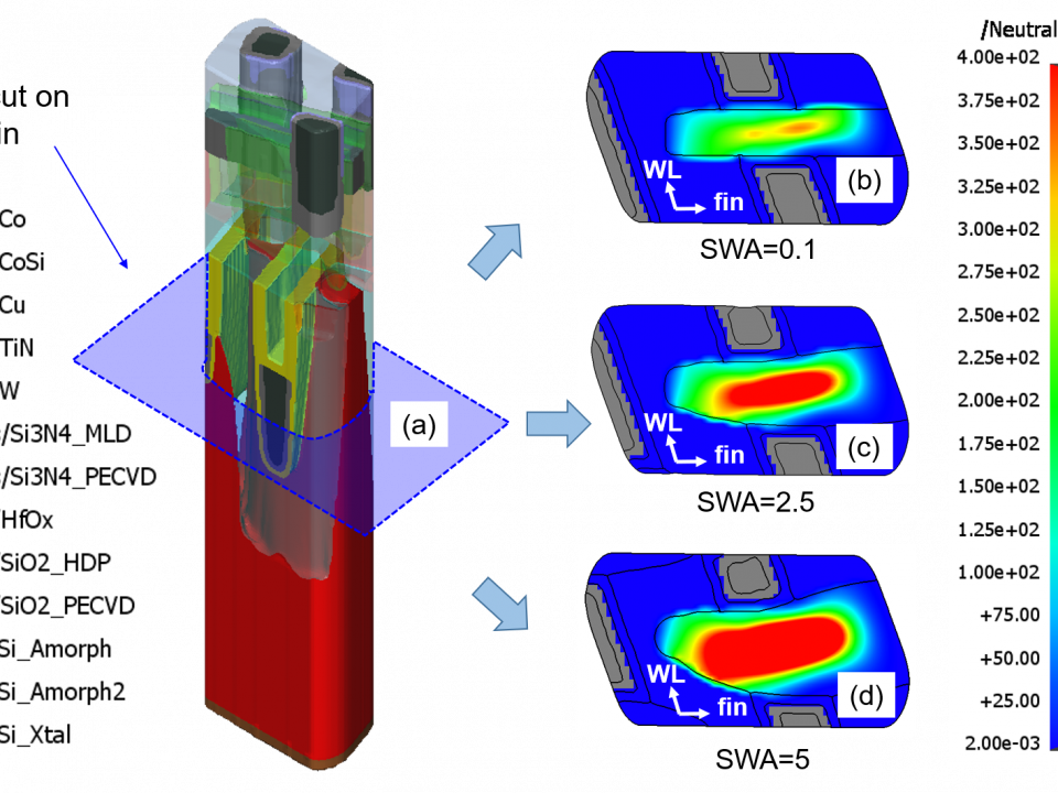
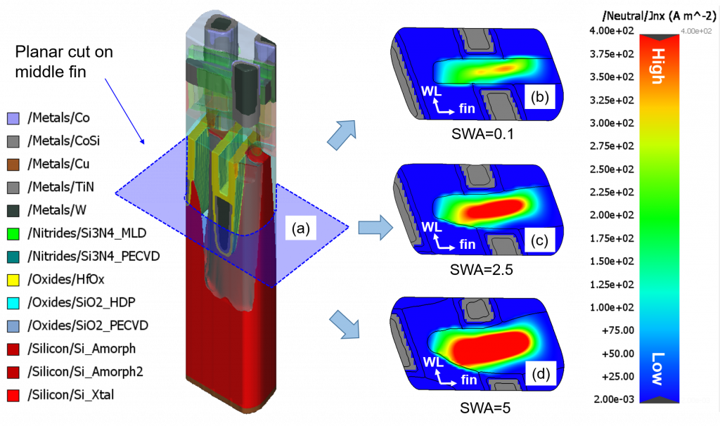
Introduction With continuing FinFET device process scaling, micro loading control becomes increasingly important due to its significant impact on yield and device performance [1-2]. Micro-loading occurs when the local etch […]
In a DRAM structure, the charging and discharging process of capacitor-based memory cells is directly controlled by the transistor [1].With transistor sizes approaching the lower limits of physical achievability, manufacturing […]
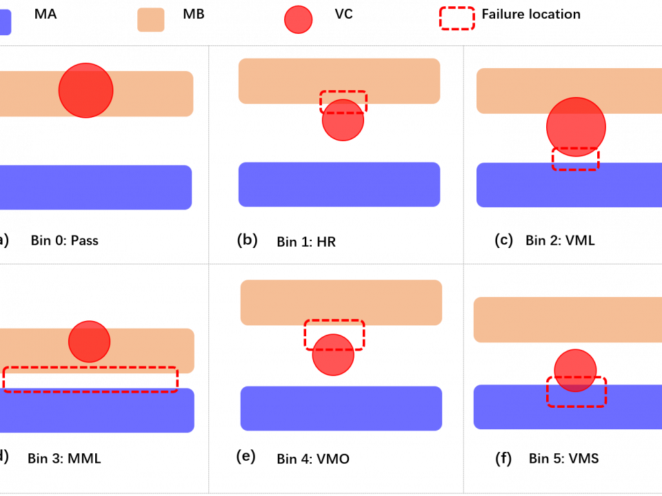
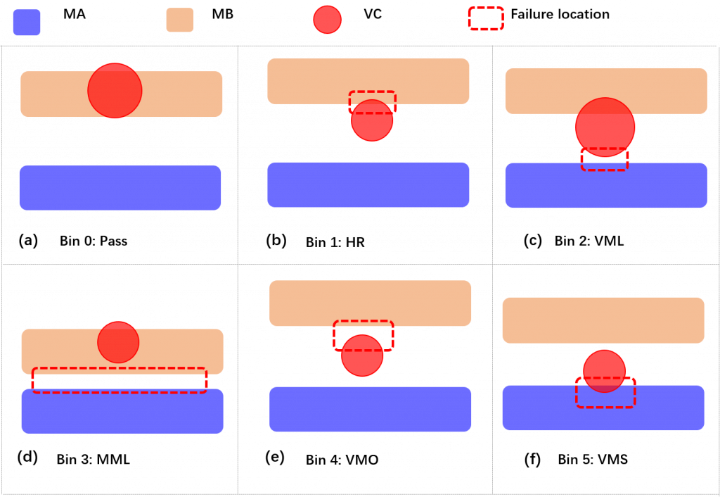
Using failure bin classification, yield prediction and process window optimization to predict and enhance yield Device yield is highly dependent upon proper process targeting and variation control of fabrication steps, […]

