Introduction Cu’s resistivity depends on its crystal structure, void volume, grain boundaries and material interface mismatch, which becomes more significant at smaller scales. The formation of Cu wires is traditionally […]
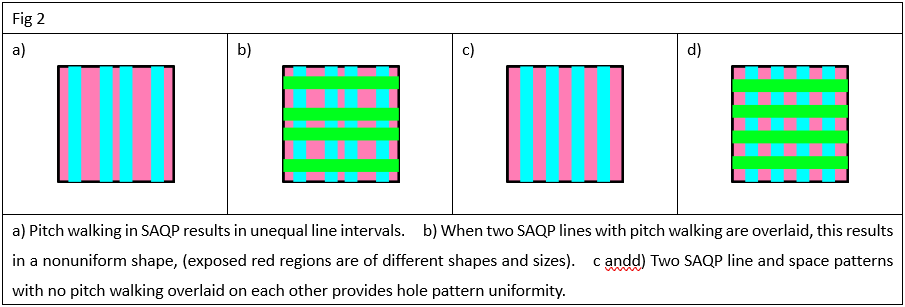
Despite the growing interest in EUV lithography, self-aligned quadruple patterning (SAQP) still holds many technical advantages in pattern consistency, simplicity, and cost. This is particularly true for very simple and […]
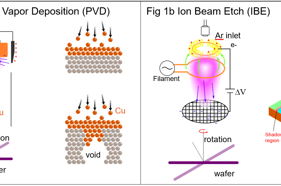
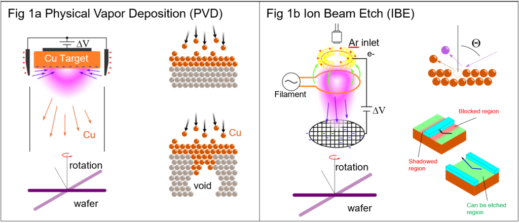
In dry etching, the trajectory of accelerated ions is non-uniform and non-vertical, due to collisions with gas molecules and other random thermal effects (Figure 1). This has an impact on […]
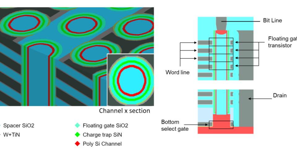
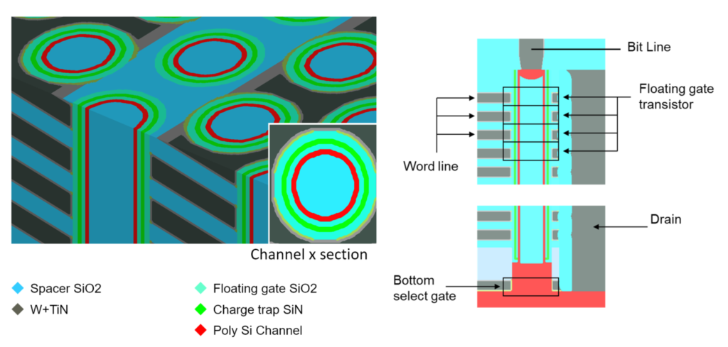
3D NAND flash memory has enabled a new generation of non-volatile solid-state storage useful in nearly every electronic device imaginable. 3D NAND can achieve data densities exceeding those of 2D NAND […]