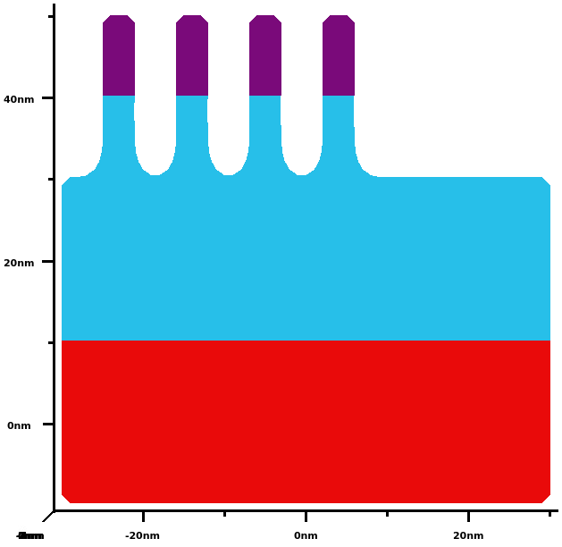
Introduction In logic devices such as FinFETs (field-effect transistors), metal gate parasitic capacitance can negatively impact electrical performance. One way to reduce this parasitic capacitance is to optimize the metal […]
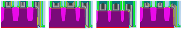
Introduction The semiconductor industry has been focused on scaling and developing advanced technologies using advanced etch tools and techniques. With decreasing semiconductor device dimensions and increases in process complexity, the […]
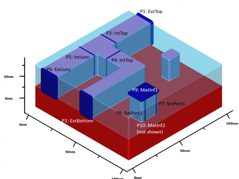
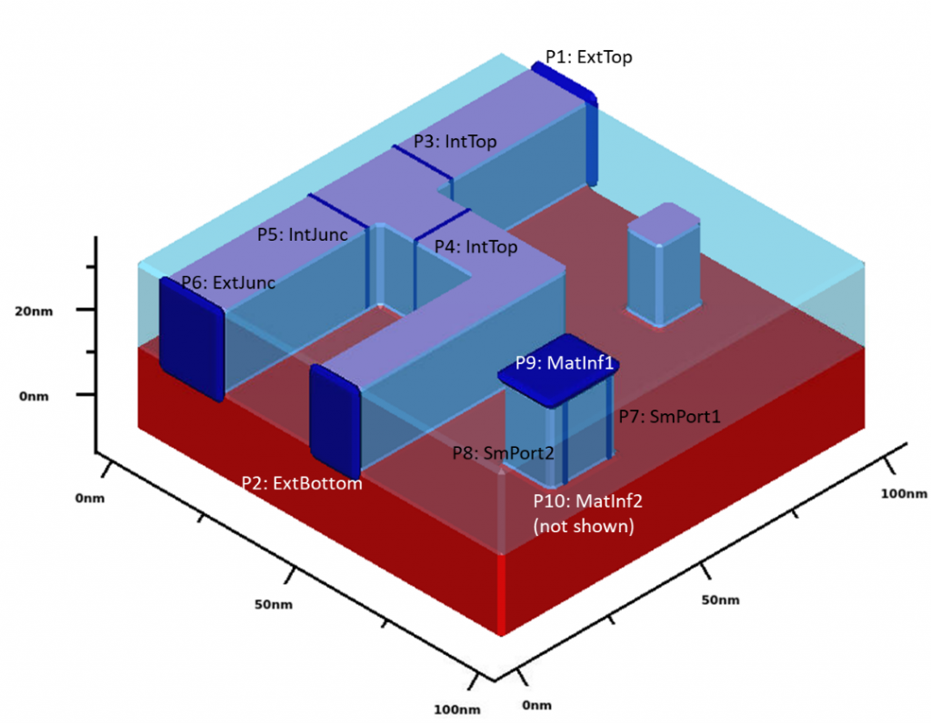
Netlist Extraction is an important SEMulator3D® capability that allows a user to extract parasitic resistance and capacitance for different line and via segments during process modeling. This detailed electrical netlist […]
Process engineers and integrators can use virtual process modeling to test alternative process schemes and architectures without relying on wafer-based testing. One important aspect of building an accurate process model […]
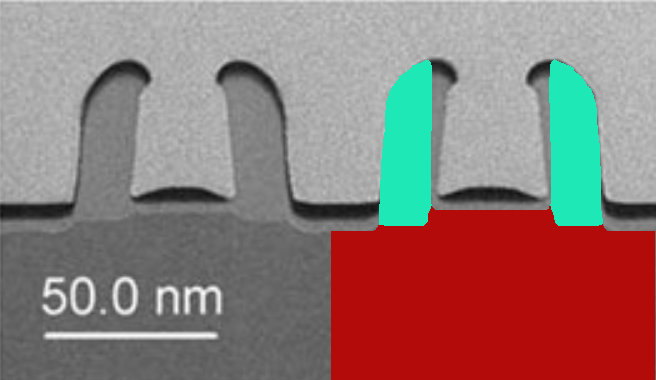
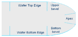
As semiconductor technology scales down in size, process integration complexity and defects are increasing in 3D NAND flash, partially due to larger stack deposits and thickness variability between the wafer […]