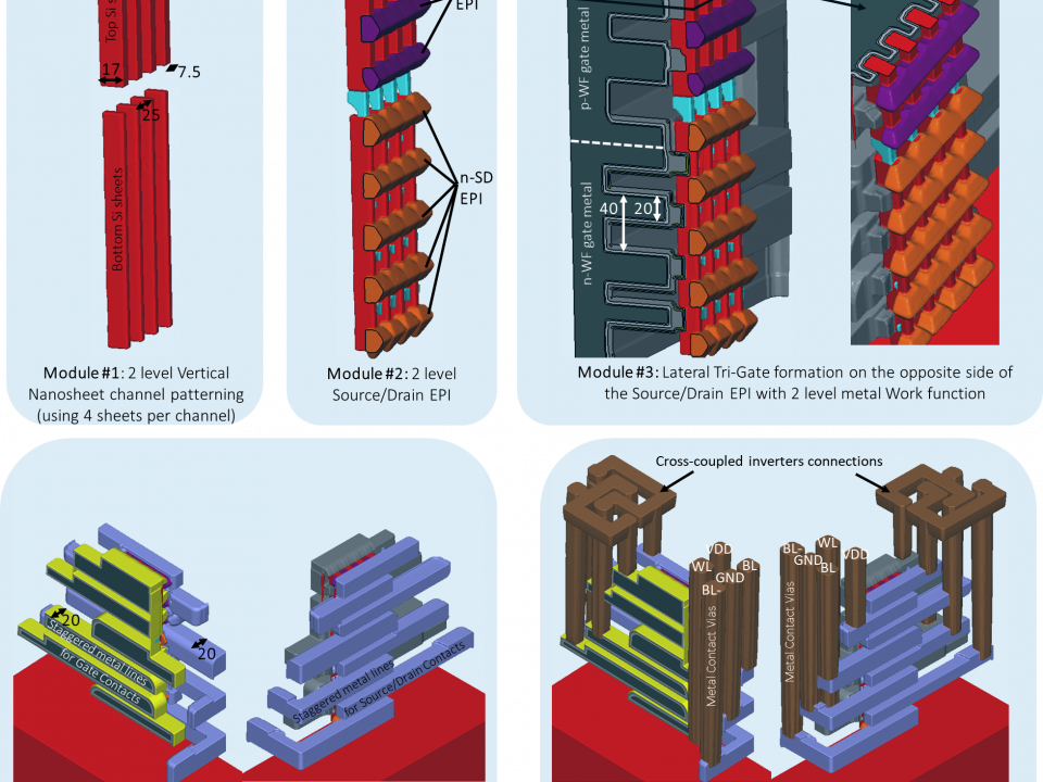
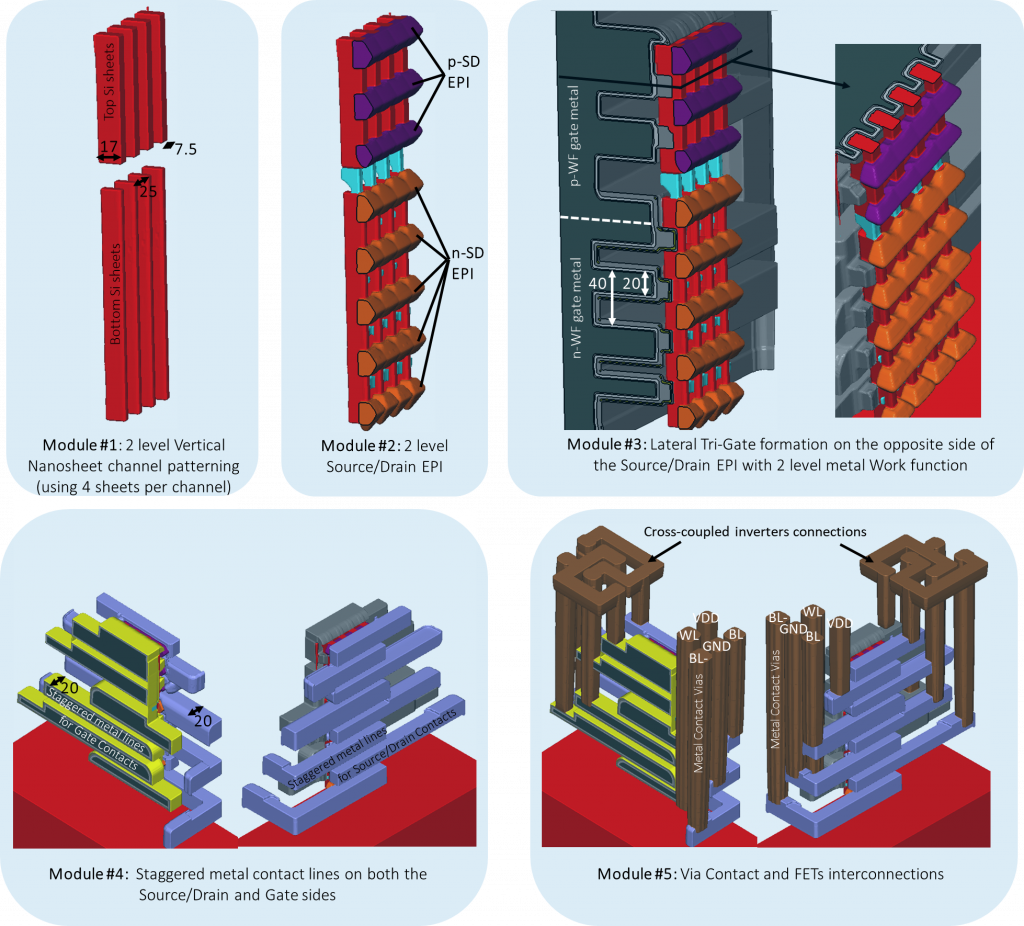
Static Random-Access Memory (SRAM) has been a key element for logic circuitry since the early age of the semiconductor industry. The SRAM cell usually consists of six transistors connected to […]
While contact gate pitch (GP) and fin pitch (FP) scaling continues to provide higher performance and lower power to FinFET platforms, controlling RC parasitics and achieving higher transistor performance at […]
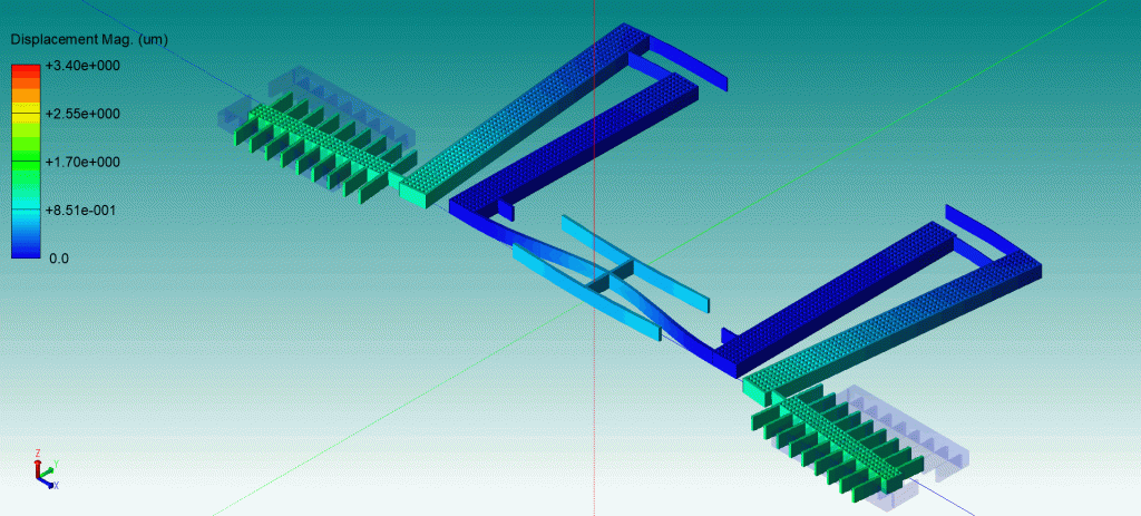
Guest Author: Jérôme Juillard, Ph.D., Professor, CentraleSupélec (Paris-Saclay University) Every year, I teach different aspects of sensors and MEMS design to about a hundred students. The pupils range from first […]
How can virtual process libraries accelerate semiconductor process development? Process engineers develop ideal solutions to engineering problems using a logical theoretical framework combined with logical engineering steps. Unfortunately, many process […]
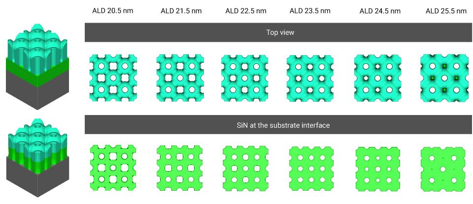
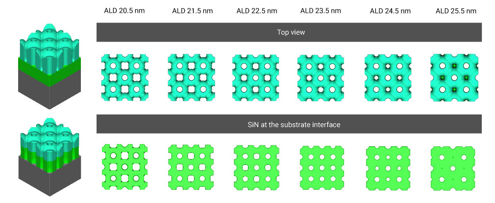
New integration and patterning schemes used in 3D memory and logic devices have created manufacturing and yield challenges. Industrial focus has shifted from the scaling of predictable unit processes in […]
Coventor’s SEMulator3D and CoventorMP MEMS Design Platform now available to startups and researchers across Canada’s National Design Network MONTREAL and FREMONT, Calif. – November 17, 2020 – Coventor®, a Lam Research Company, […]
When they were first commercialized at the 22 nm node, finFETs represented a revolutionary change to the way we build transistors, the tiny switches in the “brains” of a chip. As […]
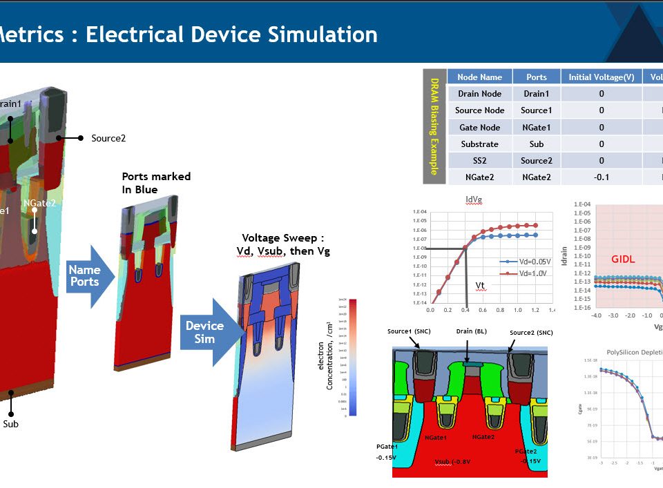
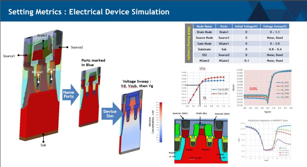
In a DRAM structure, the charging and discharging process of capacitor-based memory cells is directly controlled by the transistor [1].With transistor sizes approaching the lower limits of physical achievability, manufacturing […]
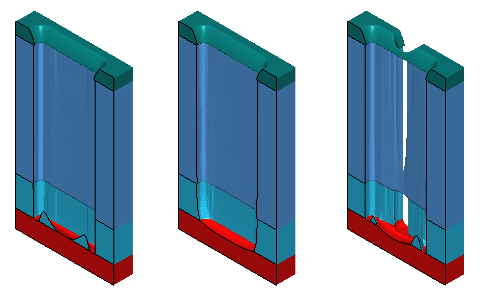
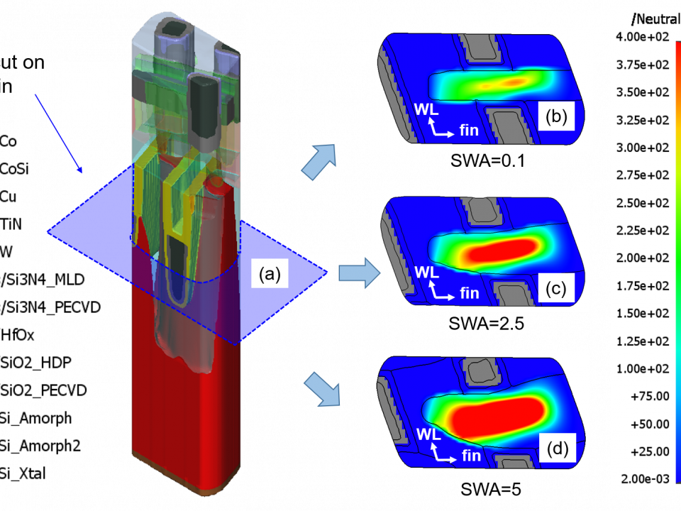
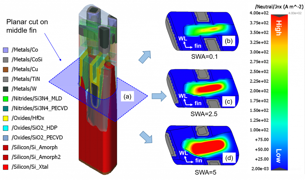
In dry etching, the trajectory of accelerated ions is non-uniform and non-vertical, due to collisions with gas molecules and other random thermal effects (Figure 1). This has an impact on […]
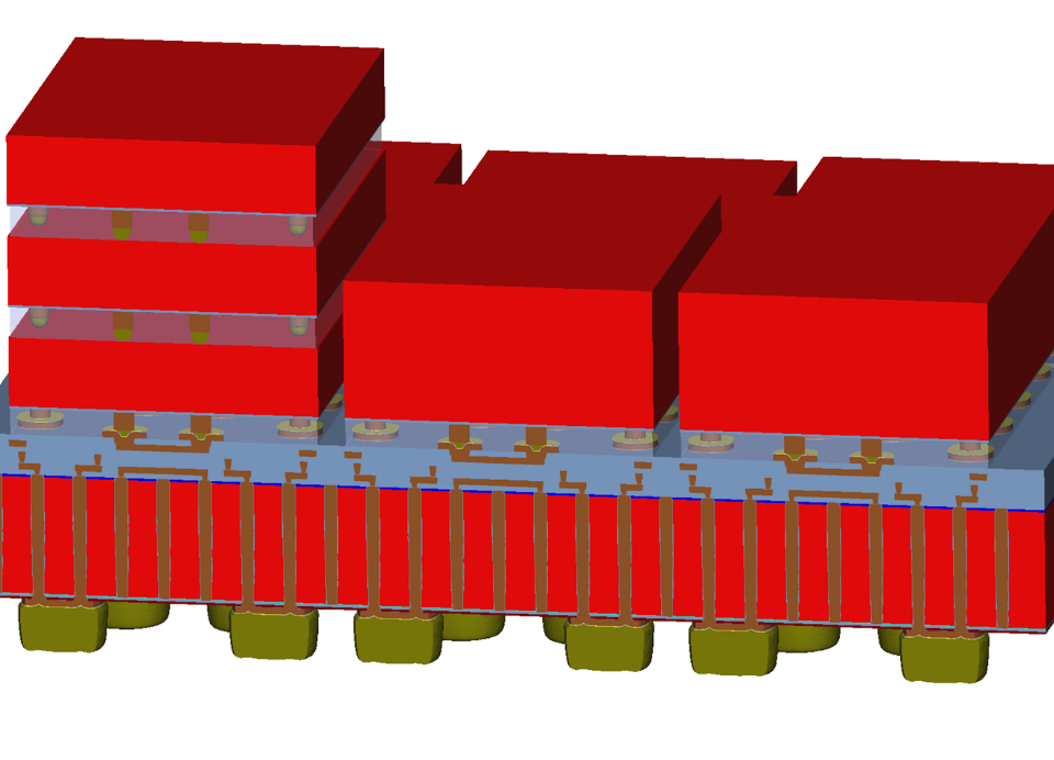
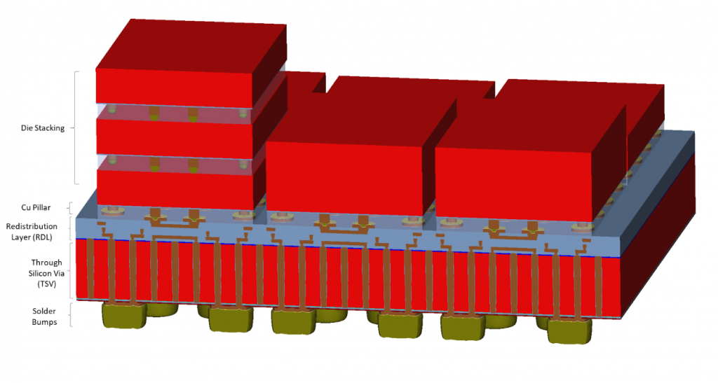
Chip packaging has expanded from its conventional definition of providing protection and I/O for a discrete chip, to encompassing a growing number of schemes for interconnecting multiple types of chips. […]

