At the beginning of my career in semiconductor equipment, the backside of the wafer was a source of anxiety. In one memorable instance in my early career, several wafers flew […]
When evaluating shrinking metal linewidths in advanced semiconductor devices, bulk resistivity is not the sole materials property for deriving electrical resistance. At smaller line dimensions, local resistivity is dominated by […]
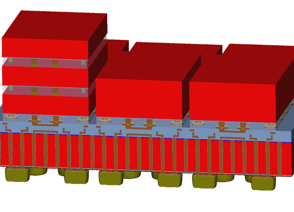
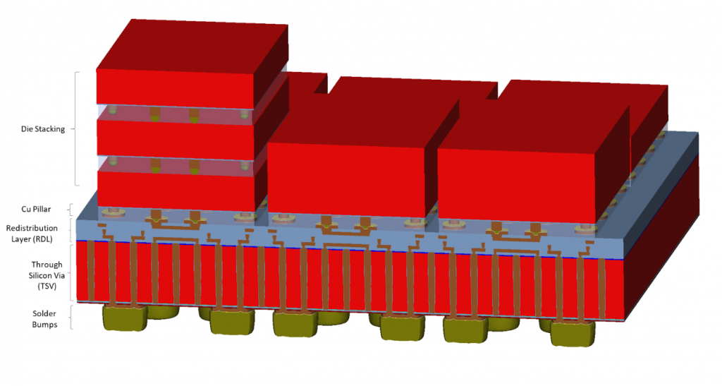
Chip packaging has expanded from its conventional definition of providing protection and I/O for a discrete chip, to encompassing a growing number of schemes for interconnecting multiple types of chips. […]
As silicon photonics manufacturing gains momentum with additional foundry and 300mm offerings, process variation issues are coming to light. Variability in silicon processing affects the waveguide shape and can result […]
With the increasing need for faster data transfer rates, the transition from electrical to optical signaling in data processing is inevitable. Copper cabling cannot keep up with the upcoming data […]
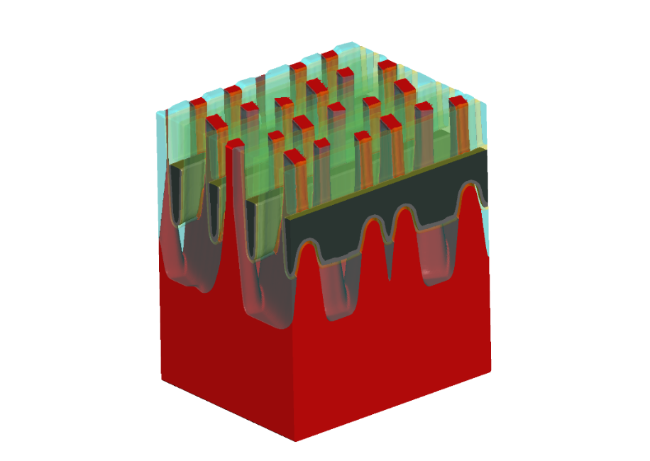
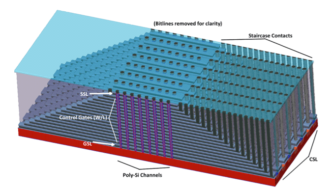
3D NAND Flash has become a hot topic in non-volatile memory these days. While planar NAND flash is still going strong, it has been increasingly difficult to scale planar technology […]
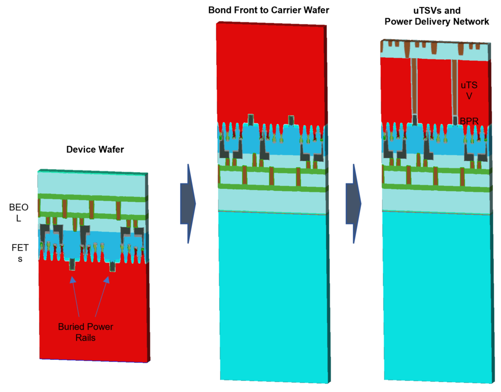
![Figure 2. Backside power delivery using buried power rails, based on [2] (not to scale).](https://www.coventor.com/wp-content/uploads/2022/12/Figure-2-December-2022-Coventor-website-blog-from-Sandy-Wen-960x720.png)